Self-assembly of Lithographically Patterned Polyhedral Nanostructures and Formation of Curving Nanostructures
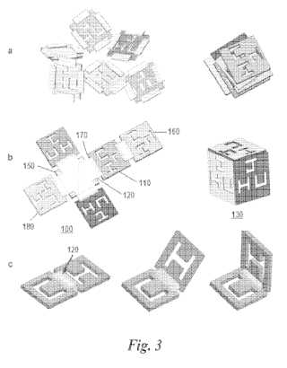
The self-assembly of polyhedral nanostructures having at least one dimension of about 100 nm to about 900 nm with electron-beam lithographically patterned surfaces is provided. The presently disclosed three-dimensional nanostructures spontaneous assemble from two-dimensional, tethered panels during plasma or wet chemical etching of the underlying silicon substrate. Any desired surface pattern with a width as small as fifteen nanometers can be precisely defined in all three dimensions. The formation of curving, continuous nanostructures using extrinsic stress also is disclosed.Attached files:
Patents:
WO 2,010,129,319
Inventor(s): GRACIAS DAVID H [US]; CHO JEONG-HYUN [US]
Type of Offer: Licensing
« More Nanotech Patents