Near-field Nano-imager
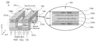
An imaging device. In one embodiment, the imaging device includes a plurality of first electrode strips in parallel to each other along a first direction x, wherein each first electrode strip has an elongated body with a first surface and an opposite, second surface and a thickness n1. The imaging device also includes a plurality of second electrode strips in parallel to each other along a second direction y that is substantially perpendicular to the first direction x, wherein each second electrode strip has an elongated body with a first surface and an opposite, second surface and a thickness n2.; The plurality of second electrode strips are positioned apart from the plurality of first electrode strips along a third direction z that is substantially perpendicular to the first direction x and the second direction y such that the plurality of first electrode strips and the plurality of second electrode strips are crossing each other accordingly to form a corresponding number of crossing points. And at each crossing point, a semiconductor component is filled between the second surface of a corresponding first electrode strip and the first surface of a corresponding second electrode strip to form an addressable pixel.Attached files:

Patents:
US 20,090,095,882
Inventor(s): LIU BOYANG [US]; HO SENG-TIONG [US]
Type of Offer: Licensing
« More Nanotech Patents
