Better Printable Electronics
 Dec-15-16
Using a novel stamping technique, MIT researchers have developed a way to create affordable interactive, printable electronic devices.
Dec-15-16
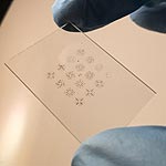
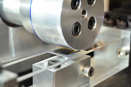
Using a novel stamping technique, MIT researchers have developed a way to create affordable interactive, printable electronic devices.According to lead MIT researcher Sanha Kim, current methods of printing electronics are limited by the size and thickness they can print, as well as the amount of detail. To overcome this obstacle, the team created a nanoporous stamp that allows a solution of nanoparticle ink to flow through it and onto the surface. The new nanoporous design enables the stamp to print clearly on an array of surfaces, and could also lead to an affordable way to manufacture large smart surfaces, such as windows or mirrors.
More Info about this Invention:
[DIGITALTRENDS.COM][NEWS.MIT.EDU]
Add Comment
Are there simple and affordable interactive whiteboards to be used at home? Persons doing remote work could scheme and communicate with it. Also children and their grandparents far away could write and draw on it together. Current large displays are still very expensive so this material could be one solution. Or any blank surface and to use a camera, a projector and electronic pens.
Posted by Uolevi Kattun on December 18, 2016
fields are required.
Comments
Are there simple and affordable interactive whiteboards to be used at home? Persons doing remote work could scheme and communicate with it. Also children and their grandparents far away could write and draw on it together. Current large displays are still very expensive so this material could be one solution. Or any blank surface and to use a camera, a projector and electronic pens.
Posted by Uolevi Kattun on December 18, 2016
Add your Comment:
[LOGIN FIRST] if you're already a member.fields are required.
Show 1 Comment