Method of Forming an Electrical Circuit Using Fullerene Derivatives
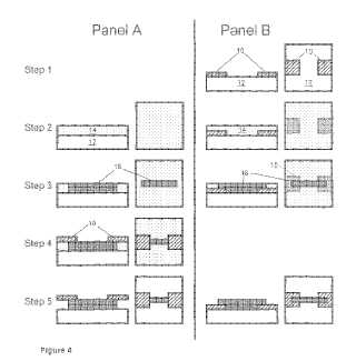
The present invention resides in a method of forming an electrical circuit, comprising forming on a substrate a non-conducting film having as its major constituent one or more fullerene derivatives, followed by exposing a selected region of said film to actinic radiation whereby to cause said selected region to become conductive. At least one electrical contact is provided (at any stage of the process) in physical contact with said selected region. The invention also reides in an electrical circuit producible by the above method.Attached files:

Patents:
WO 2,011,018,601
Inventor(s): GIBBONS FRANCIS [GB]; ROBINSON ALEX [GB]; PALMER RICHARD [GB]; PREECE JON ANDREW [GB]
Type of Offer: Sale
« More Engineering - Electrical Patents
