Nanoscale Embossing of Hetero-junction Devices
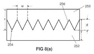
A method of manufacturing a bulk heterojunction device having a first charge transport material (250) and a second charge transport material (252). The method includes the step of forming a nanoscale relief structure (256) in the device by an embossing process. At least one of the charge transport materials (250, 252) includes an organic charge transport material. The device may be formed into an organic photo-voltaic cell.Attached files:
Patents:
WO 2,010,060,145
Inventor(s): WATKINS SCOTT EDWARD [AU]; BACH UDO [AU]; POWER GARY FAIRLESS [AU]
Type of Offer: Sale
« More Nanotech Patents