A New Type of Gapless Semiconductor Material
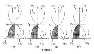
The present disclosure provides a new type of gapless semiconductor material having electronic properties that can be characterized by an electronic band structure which comprises valence and conduction band portions VB1 and CB1, respectively, for a first electron spin polarisation, and valence and conducting band portions VB2 and CB2, respectively, for a second electron spin polarisation. The valence band portion VB1 has a first energy level and one of CB1 and CB2 have a second energy level that are positioned so that gapless electronic transitions are possible between VB1 and the one of CB1 and CB2, and wherein the gapless semiconductor material is arranged so that an energy bandgap is defined between VB2 and the other one of CB1 and CB2.Attached files:
Patents:
KR 20,100,135,254
Inventor(s): WANG XIAOLIN [AU]
Type of Offer: Sale
« More Electronics Patents