Method for Encapsulating a Device in a Microcavity
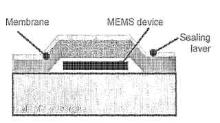
Manufacturing a semiconductor device involves forming (200) a sacrificial layer where a micro cavity is to be located, forming (210) a metal layer of thickness greater than 1 micron over the sacrificial layer, forming (220) a porous layer from the metal layer, the porous layer having pores of length greater than ten times their breadth, and having a breadth in the range 10 nm-500 nanometers. The pores can be created by anodising, electrodeposition or dealloying. Then the sacrificial layer can be removed (230) through the porous layer, to form the micro cavity, and pores can be sealed (240). Encapsulating MEMS devices with a porous layer can reduce costs by avoiding using photolithography for shaping the access holes since the sacrificial layer is removed through the porous membrane.Attached files:
Patents:
US 7,803,665
Inventor(s): WITVROUW ANN [BE]; VAN HOOF CHRIS [BE]; HELLIN RICO RAQUEL CONSUELO [ES]; MUSCAT ANTHONY JOSEPH [US]; FRANSAER JAN [BE]; CELIS J
Type of Offer: Sale
« More Electronics Patents