Method for forming MEMS devices having low contact resistance and devices obtained thereof
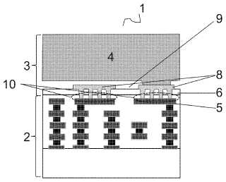
The present disclosure proposes a method for manufacturing in a MEMS device a low-resistance contact between a silicon-germanium layer and a layer contacted by this silicon-germanium layer, such as a CMOS metal layer or another silicon-germanium layer, through an opening in a dielectric layer stack separating both layers. An interlayer is formed in this opening, thereby covering at least the sidewalls of the opening on the exposed surface of the another layer at the bottom of this opening. This interlayer may comprise a TiN layer in contact with the silicon-germanium layer. This interlayer can further comprise a Ti layer in between the TiN layer and the layer to be contacted. In another embodiment this interlayer comprises a TaN layer in contact with the silicon-germanium layer. This interlayer can then further comprise a Ta layer in between the TaN layer and the layer to be contacted.Attached files:

Patents:
EP 2,277,823
Inventor(s): JAIN AJAY [US]; SEVERI SIMONE [BE]; CLAES GERT [BE]; HECK JOHN [US]
Type of Offer: Sale
« More Manufacturing Patents
