Method for fabricating a dual workfunction semiconductor device and the device made thereof
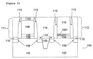
A method for manufacturing a dual work function semiconductor device and the dual work function semiconductor device made thereof is described. The method comprises providing a semiconductor substrate; providing a gate dielectric layer (104) on and in contact with the semiconductor substrate; forming a metal layer (105) on and in contact with the gate dielectric layer; forming a layer of gate filling material (106) on and in contact with the metal layer; patterning the gate dielectric layer, the metal layer and the gate filling layer to form a first gate stack and a second gate stack; selectively removing the gate filling material only from the second gate stack thereby exposing the underlying metal layer; converting the exposed metal layer into a metal oxide layer (1051).Attached files:
Patents:
EP 2,197,028
Inventor(s): ZILAN LI [BE]; TSENG JOSHUA [BE]; WITTERS THOMAS [BE]; DE GENDT STEFAN [BE]
Type of Offer: Sale
« More Electronics Patents