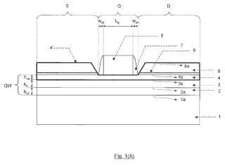
Scalable Quantum Well Device and Method for Manufacturing the Same
A quantum well device and a method for manufacturing the same are disclosed. In one aspect, the device includes a quantum well region overlying a substrate, a gate region overlying a portion of the quantum well region, a source and drain region adjacent to the gate region. The quantum well region includes a buffer structure overlying the substrate and including semiconductor material having a first band gap, a channel structure overlying the buffer structure including a semiconductor material having a second band gap, and a barrier layer overlying the channel structure and including an un-doped semiconductor material having a third band gap. The first and third band gap are wider than the second band gap. Each of the source and drain region is self-aligned to the gate region and includes a semiconductor material having a doped region and a fourth band gap wider than the second band gap.Attached files:
Patents:
US 20,090,283,756
Inventor(s): HELLINGS GEERT [BE]; ENEMAN GEERT [BE]; MEURIS MARC [BE]
Type of Offer: Sale
« More Electronics Patents