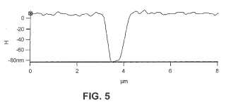
Procedure for Manufacturing Nanochannels
It comprises the following steps: (i) Depositing on glass a nickel electrode layer; (ii) depositing a layer of photosensitive material (photoresist) on the electrode layer; (iii) conferring a pattern on the photoresist having photolithographic form, covering it with a pattern mask and exposing it to light; (iv) lifting off the exposed portion of the nickel layer, forming in this manner a pattern of grooves; (v) filling such grooves with palladium by electrodeposition; (vi) removing the residual layer of photoresist and the residual layer of nickel, obtaining in this manner a master having a projecting pattern; (vii) transferring the pattern of the master to polydimethylsiloxane to obtain a moulded part; (viii) separating the moulded part and (ix) joining it to the planar covering part to cover the empty grooves. It is useful for manufacturing nanochannels having complicated and well-defined patterns of independently-controlled width and height.Attached files:
Patents:
WO 2,010,072,861
Inventor(s): GARCIA GUEELL ALEIX [ES]; SANZ CARRASCO FAUSTO [ES]
Type of Offer: Sale
« More Nanotech Patents