Thyristor radiation detector array and applications thereof
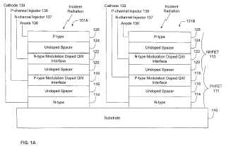
An array of thyristor detector devices is provided having an epitaxial growth structure with complementary types of modulation doped quantum well interfaces located between a P+layer and an N+ layer. The thyristor detector devices operate over successive cycles that each include a sequence of two distinct modes: a setup mode and a signal acquisition mode. During the setup mode, the n-type quantum well interface and/or p-type quantum well interface is(are) substantially emptied of charge. During the signal acquisition mode, photocurrent is generated by the thyristor detector device in response to the absorption of incident electromagnetic radiation therein, which can induce the thyristor detector device to switch from on OFF state to an ON state. The OFF/ON state of the thyristor detector device produces an output digital electrical data that corresponds to the amount of incident radiation absorbed by the thyristor detector device during the signal acquisition mode of the current cycle. In the preferred embodiment, the array of thyristor detector devices is part of a monolithic integrated circuit that includes additional electronic circuitry and/or optical components. Moreover, the array of thyristor detector devices is preferably part of a monolithic integrated circuit for high angular resolution laser irradiation detection.Attached files:
Patents:
EP 2,104,146
Inventor(s): TAYLOR GEOFF W [US]
Type of Offer: Licensing
« More Electronics Patents