Efficient Solar Cells Using All-organic Nanocrystalline Networks
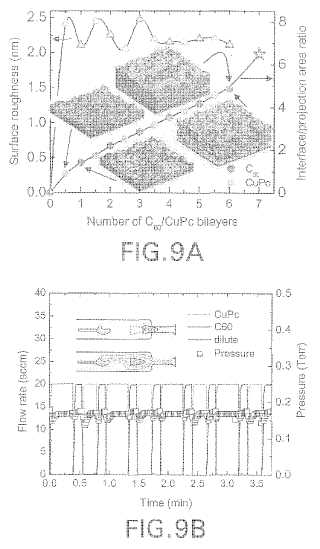
An optoelectronic device and a method of fabricating a photosensitive optoelectronic device includes depositing a first organic semiconductor material on a first electrode to form a continuous first layer; depositing a layer of a second organic semiconductor material on the first layer to form a discontinuous second layer, portions of the first layer remaining exposed; and depositing the first organic semiconductor material on the second layer to form a discontinuous third layer, portions of at least the second layer remaining exposed. The depositing of the first and second organic semiconductor materials are alternated a number of times until a final layer of the second organic material is added to form a continuous layer. A second electrode is deposited over this final layer. One of the first electrode and the second electrode is transparent, and the first organic semiconductor material is one or more donor-type materials or one or more acceptor-type materials relative to second organic semiconductor material, which is one or more materials of the other material type.Attached files:
Patents:
WO 2,009,012,324
Inventor(s): SUN KAI [US]; YANG FAN [US]; FORREST STEPHEN R [US]
Type of Offer: Licensing
« More Nanotech Patents
« More Solar Patents