Organic Triodes with Novel Grid Structures and Method of Production
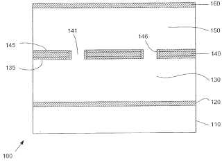
An organic semiconductor device is provided. The device has a first electrode and a second electrode, with an organic semiconductor layer disposed between the first and second electrodes. An electrically conductive grid is disposed within the organic semiconductor layer, which has openings in which the organic semiconductor layer is present. At least one insulating layer is disposed adjacent to the electrically conductive grid, preferably such that the electrically conductive grid is completely separated from the organic semiconductor layer by the insulating layer. Methods of fabricating the device, and the electrically conductive grid in particular, are also provided. In one method, openings are formed in an electrically conductive layer with a patterned die, which is then removed.; In another method, an electrically conductive layer and a first insulating layer are etched through the mask to expose portions of a first electrode. In yet another method, a patterned die is pressed into a first organic semiconductor layer to create texture in the surface of the first organic semiconductor layer, and then removed. An electrically conductive material is then deposited onto the first organic semiconductor layer from an angle to form a grid having openings as a result of the textured surface and the angular deposition. In each of the methods, insulating layers are preferably deposited or otherwise formed during the process to completely separate the electrically conductive layer from previously and subsequently deposited organic semiconductor layers.Attached files:
Patents:
US 7,943,419
Inventor(s): BALDO MARC [US]; PEUMANS PETER [US]; FORREST STEPHEN [US]; KIM CHANGSOON [US]
Type of Offer: Licensing
« More Electronics Patents