Stacked Organic Photosensitive Devices
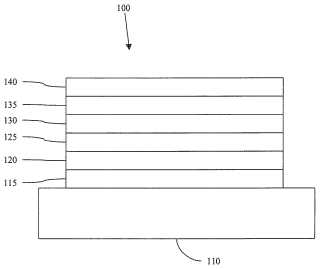
A device is provided having a first electrode, a second electrode, a first photoactive region having a characteristic absorption wavelength lambda1 and a second photoactive region having a characteristic absorption wavelength lambda2. The photoactive regions are disposed between the first and second electrodes, and further positioned on the same side of a reflective layer, such that the first photoactive region is closer to the reflective layer than the second photoactive region. The materials comprising the photoactive regions may be selected such that lambda1 is at least about 10% different from lambda2.; The device may further comprise an exciton blocking layer disposed adjacent to and in direct contact with the organic acceptor material of each photoactive region, wherein the LUMO of each exciton blocking layer other than that closest to the cathode is not more than about 0.3 eV greater than the LUMO of the acceptor material.Attached files:
Patents:
HK 1,113,227
Inventor(s): FORREST STEPHEN; JIANGENG XUE; SOICHI UCHIDA; RAND BARRY P
Type of Offer: Licensing
« More Electronics Patents