Power Junction Field Effect Power Transistor with Highly Vertical Channel and Uniform Channel Opening
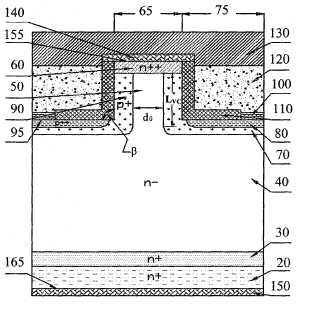
A semiconductor vertical junction field effect power transistor formed by a semiconductor structure having top and bottom surfaces and including a plurality of semiconductor layers with predetermined doping concentrations and thicknesses and comprising at least a bottom layer as drain layer, a middle layer as blocking and channel layer, a top layer as source layer. A plurality of laterally spaced U-shaped trenches with highly vertical side walls defines a plurality of laterally spaced mesas. The mesas are surrounded on the four sides by U-shaped semiconductor regions having conductivity type opposite to that of the mesas forming U-shaped pn junctions and defining a plurality of laterally spaced long and vertical channels with a highly uniform channel opening dimension. A source contact is formed on the top source layer and a drain contact is formed on the bottom drain layer. A gate contact is formed on the bottom of the U-shaped trenches for the purpose of creating and interrupting the vertical channels so as to turn on and turn off the transistor.Attached files:
Patents:
US 20,100,148,224
Inventor(s): ZHAO JIAN H [US]
Type of Offer: Licensing
« More Electronics Patents