Gallium Nitride-based Device and Method
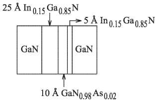
A gallium nitride-based device has a first GaN layer and a type II quantum well active region over the GaN layer. The type II quantum well active region comprises at least one InGaN layer and at least one GaNAs layer comprising 1.5 to 8% As concentration. The type II quantum well emits in the 400 to 700 nm region with reduced polarization affect.Attached files:
Patents:
US 20,090,162,963
Inventor(s): TANSU NELSON [US]; ARIF RONALD A [US]; EE YIK KHOON [US]
Type of Offer: Licensing
« More Engineering - Electrical Patents