Optical Rectification Device and Method of Making Same
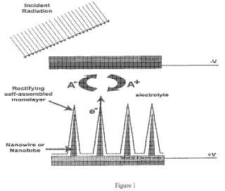
A general approach is provided for producing devices that absorb optical photons (visible to near IR) and performs charge separation with a useful voltage between holes and electrons. These holes and electrons may be collected in electrodes for performing useful work outside the device. The described technology is generally based upon rectification of plasmons (collective electric excitations) generated by absorbing light with tuned metallic antennas. According to some embodiments, the present invention provides a spatial array of nanoscale conductors forming an optical rectenna that responds to an incident light source and generates a current offset that may be rectified by a rectification-inducing material. The present inventors foresee an extensive use of these optical rectennas as photovoltaic devices, as well as a wide interest in diverse fundamental research and applied technologies.Attached files:
Patents:
US 20,110,100,440
Inventor(s): SCHMIDT HOWARD K [US]; DUQUE JUAN [US]
Type of Offer: Licensing
« More Optical Science Patents