Semiconductor Device and Method
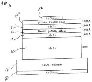
The present invention is directed to a semiconductor device that includes at least one p-n junction including a p-type material, an n-type material, and a depletion region. The at least one p-n junction is configured to generate bulk photocurrent in response to incident light. The at least one p-n junction is characterized by a conduction band energy level, a valence band energy level and a surface Fermi energy level. The surface Fermi energy level is pinned either near or above the conduction band energy level or near or below the valence band energy level. A unipolar barrier structure is disposed in a predetermined region within the at least one p-n junction. The unipolar barrier is configured to raise the conduction band energy level if the surface Fermi energy level is pinned near or above the conduction band energy level or lower the valence band energy level if the surface Fermi energy level is pinned near or below the valence band energy level such that the unipolar barrier is configured to propagate the bulk photocurrent and substantially block surface leakage current. The at least one p-n junction and the unipolar barrier are integrally formed.Attached files:
Patents:
US 20,100,230,720
Inventor(s): WICKS GARY W [US]
Type of Offer: Licensing
« More Electronics Patents