Cmos Image Sensor on Stacked Semiconductor-on-insulator Substrate and Process for Making Same
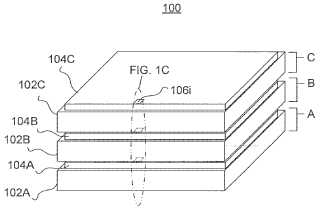
Methods and apparatus for producing a CMOS image sensor result in a plurality of photo sensitive layers (A,B,C ); each layer including: a glass or glass ceramic substrate (102A, 102B, 102C) having first (102A-1, 102B-1, 102C-19 and second (102A-2, 102B-2, 102C-2) spaced-apart surfaces; a semiconductor layer (104A, 104B, 104C) disposed on the first surface of the glass or glass ceramic substrate; and a plurality of pixel structures formed in the semiconductor layer, each pixel structure including a plurality of semiconductor islands, (104A-1, 104A-2, 104B-1, 104B-2, 104C-1, 104C-2) at least one island operating as a color sensitive photo-detector sensitive to a respective range of light wavelengths, wherein the plurality of photo sensitive layers (A, B, C) are stacked one on the other, such that incident light enters the CMOS image sensor through the second spaced-apart surface (102A-2) of the glass or glass ceramic substrate (102A) of one (A) of the plurality of photo sensitive layers, (A, B, C) and subsequently passes into further photo sensitive layers (B, C) if one or more wavelengths of the incident light are sufficiently long.Attached files:
Patents:
WO 2,010,127,070
Inventor(s): BOCKO MARK F [US]; IGNJATOVIC ZELJKO [US]; KOSIK-WILLIAMS CARLO [US]; WALTON DONNELL T [US]; WANG CHUANCHE [US]; ZAVISLAN JAMES
Type of Offer: Licensing
« More Medical Devices Patents