Collections of Laterally Crystallized Semiconductor Islands for Use in Thin Film Transistors
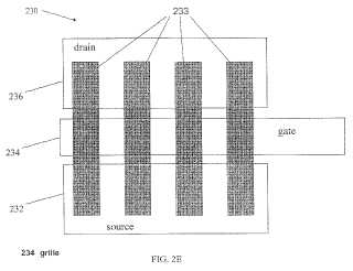
Collections of laterally crystallized semiconductor islands for use in thin film transistors and systems and methods for making same are described. A display device includes a plurality of thin film transistors (TFTs) on a substrate, such that the TFTs are spaced apart from each other and each include a channel region that has a crystalline microstructure and a direction along which a channel current flows. The channel region of each of the TFTs contains a crystallographic grain that spans the length of that channel region along its channel direction. Each crystallographic grain in the channel region of each of the TFTs is physically disconnected from and crystallographically uncorrelated with each crystallographic grain in the channel region of each adjacent TFT.Attached files:
Patents:
US 20,110,108,843
Inventor(s): IM JAMES S [US]; CHUNG UI-JIN [US]
Type of Offer: Licensing
« More Crystallography Patents
« More Electronics Patents