Processes for Fabricating All-back-contact Heterojunction Photovoltaic Cells
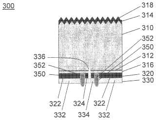
Processes for fabricating back contacts for photovoltaic cell devices are disclosed. The processes involve depositing a passivation layer on the back surface of a wafer, depositing an emitter layer on the passivation layer, depositing a metal layer on the emitter layer, laser firing selected areas of the metal layer to form base contacts, laser cutting the metal layer to create at least one isolation region between emitter contacts and base contacts, and applying a stream of reactive gas to form a second passivation layer in the isolation region. The process may further involve inkjetting a resist on the passivation layer in a pattern corresponding to a boundary between the one or more emitter contacts and the one or more base contacts, and laser cutting the metal layer over the resist to create the isolation region.Attached files:

Patents:
US 20,100,319,769
Inventor(s): BIRKMIRE ROBERT W [US]; HEGEDUS STEVEN S [US]; DAS UJJWAL K [US]
Type of Offer: Sale
« More Solar Patents
