Light emitting and lasing semiconductor devices and methods
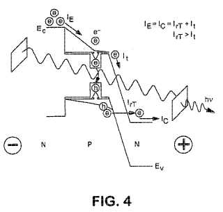
A two terminal semiconductor device for producing light emission in response to electrical signals, includes: a terminal-less semiconductor base region disposed between a semiconductor emitter region and a semiconductor collector region having a tunnel junction adjacent the base region; the base region having a region therein exhibiting quantum size effects; an emitter terminal and a collector terminal respectively coupled with the emitter region and the collector region; whereby application of the electrical signals with respect to the emitter and collector terminals, causes light emission from the base region. Application of the electrical signals is operative to reverse bias the tunnel junction. Holes generated at the tunnel junction recombine in the base region with electrons flowing into the base region, resulting in the light emission.; The region exhibiting quantum size effects is operative to aid recombination.Attached files:
Patents:
US 7,953,133
Inventor(s): HOLONYAK JR NICK [US]; FENG MILTON [US]; WALTER GABRIEL [US]; JAMES ADAM [US]
Type of Offer: Licensing
« More Electronics Patents