Method of Plasma Etching Ga-based Compound Semiconductors
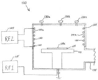
A method of plasma etching Ga-based compound semiconductors includes providing a process chamber and a source electrode adjacent to the process chamber. The process chamber contains a sample comprising a Ga-based compound semiconductor. The sample is in contact with a platen which is electrically connected to a first power supply, and the source electrode is electrically connected to a second power supply. The method includes flowing SiCl4 gas into the chamber, flowing Ar gas into the chamber, and flowing H2 gas into the chamber. RF power is supplied independently to the source electrode and the platen. A plasma is generated based on the gases in the process chamber, and regions of a surface of the sample adjacent to one or more masked portions of the surface are etched to create a substantially smooth etched surface including features having substantially vertical walls beneath the masked portions.Attached files:
Patents:
US 20,100,159,706
Inventor(s): QIU WEIBIN [US]; GODDARD LYNFORD L [US]
Type of Offer: Licensing
« More Electronics Patents