Transistor Device and Method
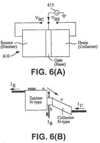
A field-effect transistor device, including: a semiconductor heterostructure comprising, in a vertically stacked configuration, a semiconductor gate layer between semiconductor source and drain layers, the layers being separated by heterosteps; the gate layer having a thickness of less than about 100 Angstroms; and source, gate, and drain electrodes respectively coupled with said source, gate, and drain layers. Separation of the gate by heterosteps, rather than an oxide layer, has very substantial advantages.Attached files:
Patents:
WO 2,009,051,663
Inventor(s): FENG MILTON [US]; HOLONYAK NICK JR [US]
Type of Offer: Licensing
« More Electronics Patents