Wet Etching Process
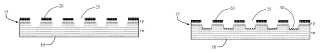
The present invention illustrates a bulk silicon etching technique that yields straight sidewalls, through wafer structures in very short times using standard silicon wet etching techniques. The method of the present invention employs selective porous silicon formation and dissolution to create high aspect ratio structures with straight sidewalls for through wafer MEMS processing.Attached files:
Patents:
US 7,892,440 issued 2011-02-22 [MORE INFO]
Inventor(s): BHANSALI SHEKHAR [US]; RAHMAN ABDUR RUB ABDUR [US]; KEDIA SUNNY [US]
Type of Offer: Licensing
« More Material Science Patents