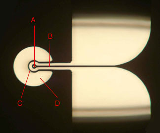
Transmission Electron Microscope Phase-contrast Enhancement
APPLICATIONS OF TECHNOLOGY:High-contrast electron microscopy, especially for radiation-sensitive materials and weak phase objects like:
whole-mount subcellular organelles and thin areas of whole cells isolated biological macromolecules thin crystals thin sections of cells and tissues Single-particle averaging for low molecular weight macromolecules Tomographic imaging of 1.5 – 2 nm features
ADVANTAGES:
Obtains high contrast images of weak phase objects Provides uniform contrast for all ranges of resolution Uses all scattered electrons Allows quantitative interpretation of an object's structure
ABSTRACT:
Berkeley Lab scientists have invented a practical solution to the problem of obtaining uniform phase contrast for transmission electron microscopy – a problem that has been practically intractable since electron microscopy was invented in 1931.
Robert Glaeser and Jian Jin have developed an apparatus that can be integrated into transmission electron microscopes (TEMs) to enable high contrast imaging of weak phase objects without the need to defocus the image. Weak phase objects include biological specimens, thin specimens of polymers and other organic materials, and various inorganic materials under certain imaging conditions.
The standard method for obtaining high quality images of these objects requires operating the microscope in an out-of-focus condition. This practice introduces unwanted contrast reversals at high spatial frequency or resolution. These contrast reversals become increasingly severe as one strives to generate better contrast at low spatial frequency. The new Berkeley Lab invention will provide high levels of contrast across all ranges of resolution using all the scattered electrons.
The TEM phase element also enables tomographic imaging of 1.5-2 nm features and single-particle averaging for macromolecules with molecular weights as low as 100,000 daltons.
The inventors use a microfabricated, two-electrode electrostatic device to selectively apply a 90 degree phase shift to the central, unscattered beam in the back focal plane of the objective lens of an electron microscope. The device is essentially a shielded drift tube down the center of which electrons travel for several micrometers at a constant electrostatic potential.
Engineering challenges overcome by this invention include precision micrometer fabrication, preventing electrostatic charging and contamination of the phase element device, and keeping the central hole of the electron optical element centered on and axially aligned with the unscattered electron beam.
Attached files:

Inventor(s): Robert Glaeser and Jian Jin
Type of Offer: Licensing
« More Nanotech Patents
