Brighter Organic Light Emitting Diodes
BACKGROUND: Triplet emitters are promising materials for creating bright organic light emitting diodes (OLEDs). Iridium (Ir) organometallic complexes are especially attractive because of their high quantum yield of phosphorescence and their tunability over a broad emissive spectral range. However, at high carrier injection rates, saturation of emissive states and triplet-triplet quenching limits OLED performance. Thus, there is a need to accelerate Ir radiative decay in OLEDs while keeping other optical properties unperturbed.DESCRIPTION: University of California (UC) scientists have designed OLEDs that accelerate Ir radiative decay via an interaction of the chromophore with two-dimensional oscillations of electronic density arising from surface plasmon polaritons (SP) in metal structures. Although SP-assisted acceleration of Ir radiative decay requires a difficult balancing of several dynamical processes, the UC scientists developed two successful design strategies for meeting this challenge.
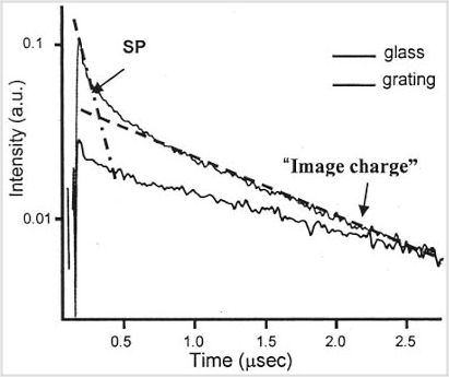
The first strategy features periodically modulated planar layers of a certain metal and of a certain transparent dielectric material. In this structure, emission decay rates are significantly faster than is the case for chromophores being deposited on a plain glass substrate (see figure 1). Part of this is due to a fast SP-assisted burst of photons, and the rest due to constructive interference between light emitted by chromophores and light reflected by the metal surface (the “image charge” effect). The acceleration of Ir radiative decay in this system can be very efficient. Integrating the data in figure 1, one finds that 56% of excited chromophores in the modulated grating have already created light quanta 1 µsec after excitation, while only 34% have done so in the ordinary glass substrate.
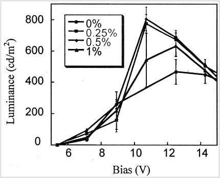
The second strategy takes advantage of the SP characteristics of spherical nanoparticles made of another metal. Unlike planar devices, these spherical metal nanoparticles do not need any special coupling to make the SP interact with radiation. The spectral position of the SP in them can be adjusted by simple variations of nanoparticle diameter and dielectric properties of the surrounding organic matrix. As can be seen in figure 2, one can then optimize brightness as a function of nanoparticle density and bias voltage. At bias voltages in the 9–12 V range, OLEDs with optimized nanoparticle densities are almost twice as bright as OLEDs without nanoparticles. This enhanced brightness can’t be attributed to increases in charge injection rate, since current densities are identical for both the doped and undoped structures under the same driving voltage. Instead, it is a product of an increased radiative decay rate and an increased quantum yield.
Emission decays on glass and on modulated metal surfaces. FIGURE 1—Emission decays on glass and on modulated metal surfaces; the modulated grating shows greater intensity due to SP-assisted photon emissions and “image charge” effects.
Brightness vs. bias voltage for various SP nanoparticle loads. FIGURE 2—Brightness as a function of bias voltage for various SP nanoparticle loads (% weight of nanoparticles relative to Ir chromophores).
APPLICATIONS: OLEDs have the potential to revolutionize flat panel and other thin-film information displays. Ease of processibility, light weight, low power consumption, resistance to shock, and use of inexpensive materials and fabrication techniques gives OLEDs a strong competitive position in this market, with this invention further strengthening OLED's advantages. Recent studies suggest that OLEDs will replace LCDs within a few years as the dominant display technology in devices which could have sales on the order of tens of billions of dollars per year. Other optoelectronic and lighting applications might also benefit from improved OLED technology.
ADVANTAGES: This invention offers two practical approaches for SP-assisted acceleration of Ir decay, with potentially significant improvements in OLED brightness.
REFERENCE: 2003-545
Attached files:
Patents:
US 6,999,222 [MORE INFO]
Type of Offer: Licensing
« More Material Science Patents
« More Optical Science Patents