Wafer Level Package Structure, and Sensor Device Obtained from the Same Package Structure
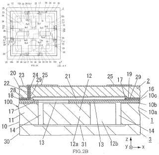
A wafer level package structure with a plurality of compact sensors such as acceleration sensors and gyro sensors is provided. This package structure is composed of a semiconductor wafer with plural sensor units, and a pair of package wafers bonded to both surfaces of the semiconductor wafer. Each of the sensor units has a frame having an opening, a movable portion held in the opening to be movable relative to the frame, and a detecting portion for outputting an electric signal according to a positional displacement of the movable portion. Since the semiconductor wafer is bonded to each of the package wafers by a solid-phase direct bonding without diffusion between a surface-activated region formed on the frame and a surface-activated region formed on the package wafer, it is possible to prevent that variations in sensor characteristics occur due to residual stress at the bonding interface.The present invention relates to a wafer level packaging technique for manufacturing compact sensor devices such as an acceleration sensor and a gyro sensor.
A primary concern of the present invention is to provide a wafer level package structure capable of providing compact sensor devices having small variations in sensor characteristics, which is formed by bonding a semiconductor wafer with a plurality of compact sensor elements such as acceleration sensors and gyro sensors to a package wafer without almost causing residual stress at the bonding interface.
Attached files:
Patents:
JP 2,006,323,453 [MORE INFO]
Inventor(s): OKUDO TAKAFUMI [JP]; SUZUKI YUJI [JP]; TAKEGAWA YOSHIYUKI [JP]; BABA TORU [JP]; GOTOU KOUJI [JP]; MIYAJIMA HISAKAZU [JP]; KATAOK
Type of Offer: Sale
« More Manufacturing Patents