Semiconductor Device for Emitting Light
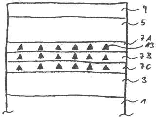
A semiconductor device according to the invention for emitting light when a voltage is applied includes a first ( 3 ), a second ( 5 ) and a third active semiconductor region ( 7 A- 7 C). While the conductivity of the first semiconductor region ( 3 ) is based on charge carriers of a first conductivity type, the conductivity of the second semiconductor region ( 5 ) is based on charge carriers of a second conductivity type, which have a charge opposite to the charge carriers of the first conductivity type The active semiconductor region ( 5 13 ) is arranged between the first and the second semiconductor regions ( 3, 5 ). Embedded in the active semiconductor region ( 5 ) are quantum structures ( 13 ) which are made from a semiconductor material which has a direct band gap. In that respect the term quantum structures is used to denote structures which in at least one direction of extent are of a dimension which is so small that the properties of the structure are substantially also determined by quantum-mechanical processes.Attached files:
Patents:
US 20,070,210,315
Inventor(s): MASSELINK WILLIAM T [DE]; HATAMI FARIBA [US]
Type of Offer: Sale
« More Engineering - Electrical Patents