Wide band gap semiconductor device including junction field effect transistor
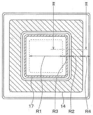
A wide band gap semiconductor device has a transistor cell region, a diode forming region, an electric field relaxation region located between the transistor cell region and the diode forming region, and an outer peripheral region surrounding the transistor cell region and the diode forming region. In the transistor cell region, a junction field effect transistor is disposed. In the diode forming region, a diode is disposed. In the electric field relaxation region, an isolating part is provided. The isolating part includes a trench dividing the transistor cell region and the diode forming region, a first conductivity-type layer disposed on an inner wall of the trench, and a second conductivity-type layer disposed on a surface of the first conductivity-type layer so as to fill the trench. The first conductivity-type layer and the second conductivity-type layer provide a PN junction.Attached files:
Patents:
US 20,100,025,693
Inventor(s): MALHAN RAJESH KUMAR [JP]; TAKEUCHI YUUICHI [JP]; RASHID JEREMY [GB]
Type of Offer: Sale
« More Engineering - Electrical Patents