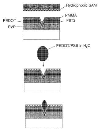
Method for Forming an Electronic Device in Multi-layer Structure
A method for forming an organic or partly organic switching device, comprising: depositing layers of conducting, semiconducting and/or insulating layers by solution processing and direct printing; defining microgrooves in the multilayer structure by solid state embossing; and forming a switching device inside the microgroove.Attached files:
Patents:
US 20,100,051,916
Inventor(s): SIRRINGHAUS HENNING [GB]; FRIEND RICHARD HENRY [GB]; STUTZMANN NATALIE [NL]; SMITH PAUL [CH]
Type of Offer: Sale
« More Nanotech Patents
« More Engineering - Electrical Patents