Light Emitting Semiconductor Methods and Devices
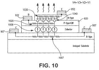
A method for producing light emission from a two terminal semiconductor device with improved efficiency, includes the following steps: providing a layered semiconductor structure including a semiconductor drain region comprising at least one drain layer, a semiconductor base region disposed on the drain region and including at least one base layer, and a semiconductor emitter region disposed on a portion of the base region and comprising an emitter mesa that includes at least one emitter layer; providing, in the base region, at least one region exhibiting quantum size effects; providing a base/drain electrode having a first portion on an exposed surface of the base region and a further portion coupled with the drain region, and providing an emitter electrode on the surface of the emitter region; applying signals with respect to the base/drain and emitter electrodes to obtain light emission from the base region; and configuring the base/drain and emitter electrodes for substantial uniformity of voltage distribution in the region therebetween. In a further embodiment lateral scaling is used to control device speed for high frequency operation.Attached files:
Patents:
WO 2,010,120,372
Inventor(s): WALTER GABRIEL [US]; FENG MILTON [US]; HOLONYAK NICK [US]; THEN HAN WUI [MY]; WU CHAO-HSIN [US]
Type of Offer: Licensing
« More Electronics Patents