Wide Band-gap Nanostructures
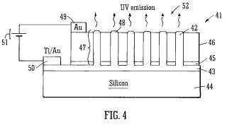
A light emitting or detecting device (41) with a substrate (44) with a surface, an array of elongate nanostructures (42) having a first end supported by the substrate (44), and a second free end projecting away from the surface; a thin insulating layer (45) formed on the surface and about the nanostructures, the insulating layer being arranged so that a substantial portion (47) of the nanostructures (42) extend through the insulating layer (45). The device allows for greater contact between the nanostructures (42) and a p-type layer (46) above the insulator and surrounding the nanostructures improving the efficiency of the device. One suitable material is ZnO.Attached files:

Patents:
WO 2,009,106,636
Inventor(s): MCGLYNN ENDA [IE]; THANGAVELU RAJENDRA KUMAR RAMA [IN]
Type of Offer: Sale
« More Nanotech Patents