Electronics Patents for Sale or License
Notify me of New Entries on this Page
You can receive an email whenever a new patent is added to this category. You can unsubscribe at any time.
New Revolutionary Heads Up Display Glasses Competing With Google
The new revolutionary Heads Up Display Glasses (HUD) competing with google, the revolutionary device that seamlessly streams notifications and text messages into your field of vision, and looks just like a regular pair of glasses.
There are loads of PROVEN opportunities for this patent, with many...
...
APPLIANCE IRON FOR MAKING EDIBLE SPOONS
Designed like an electric waffle iron, The Edible Spoon Maker lets you bake delicious, edible spoons that you can eat with any meal. It uses store-bought dough or homemade recipes and you can add virtually any ingredient for that extra pop of flavor. Just cut out each spoon shape with the included d...
...
Skateboard Lighting Apparatus
A lighting apparatus for use with a skateboard includes a light housing having top, bottom, and side walls defining an interior space. A fastener on the housing top wall is selectively attached to a lower surface of the skateboard. A plurality of lights is positioned in the light housing. A battery ...
...
Mini Notched Turbine Generator
The invention has applications in the field of wireless self-powered
micro and nano devices. It can be used as a charging system for
micro and nano batteries, and as a power supply integrated in multiple
applications such as artificial organs, valves, sensors, micro
motors and micro robots....
...
Metal-Organic Materials (MOMs) for CO2 Absorption and Methods of Using MOMs
This system exhibits permanent porosity and can be used in humid conditions to separate
components in a gas. MOMs are porous crystalline materials known for their ability to exploit equilibrium, kinetic selectivity, size selectivity, and targeted molecular recognition. They are therefore attractive...
...
Threshold Voltage Defined Switches for Programmable Camouflage Gates
Disclosed are various embodiments providing circuitry that includes camouflaged gates that each have multiple switches arranged in a predefined format. A switch at a specific position in one camouflaged gate can have a different threshold voltage than a switch at the specific position in another cam...
...
Thin Flexible RFID/NFC device on Metal
That is the only solution to achieve thin thickness to Applications where RF/NFC/RFID Antenna & Electronics :
– are applied on face of Metallic Item or any other Device (PC, Tablet, Mobile, PDA…),
– are applied within Metallic Item or any other Device (PC, Tablet, Mobile, PDA, CD, DVD…),
– are ap...
...
Remote Power State Detector
REMOTE POWER STATE DETECTOR patent us 9390600 for home or business
http://www.mysafetykitchen.com/
A system for remotely indicating a power state (ON-OFF) of a home appliances This system is easily configurable and flexible tool for smart home security systems and provides a universal and ...
...
Omni-directional Remote-controlled Mobility Apparatus
An omnidirectional mobility apparatus. The current invention is an omni-directional, remote-controlled mobility apparatus, similar to a wheelchair, which allows the transport of an individual or object(s). The device includes a cubic-shaped base with wheel wells on each vertical side of said base. W...
...
Systems and Methods for Determining a Cardiovascular Condition of a Subject
The present invention provides a Diversity Coding--Orthogonal Frequency Division Multiplexing (DC-OFDM) system and method that applies diversity coding to OFDM-based systems and provides improved probability of successful reception at the receiver and transparent self-healing and fault-tolerance. Di...
...
Electronic Traveling Suitcase
The Electronic Traveling Suitcase includes :
1) A self weighing feature that displays its weight in Pounds or Kilograms on LCD sceen.
2) Identfy and password are provided in LC D .
3) A lock which can be digitally programmed.
4) An electric motor powers wheels. The motor is powered by rechargea...
...
Electronic Mailbox System
An electronic mailbox system features: a mailbox housing with an inner cavity and slot for holding mail, a lid, an electrically-operable lock system for the lid, a mail sensor for detecting the mail being inserted into the slot, a first transmitter, a first receiver and a mailbox microprocessor; and...
...
Electrolysis Cell for Hydrogen
Apparatus for the electrolysis of hydrochloric acid having an HCl concentration in the range from 10 to 25% by weight, having an electrode chamber (A) having a cathode (1) and a further electrode chamber (B) having an anode (2), with electrode chamber (A) and electrode chamber (B) being separated by...
...
3D Forward Looking Sonar Apparatus
USA Patent - 8,717,847,B2
UK Patent - GB2500246B
UK Patent - GB2509644B
With the Echopilot 3D FLS (Forward Looking Sonar) you can see all the contours of the sea bed spread out in front of you, colour coded with red being dangerously shallow, and refreshed so fast that you can keep your speed. ...
...
Movable Cable Connectors
These patents cover CABLE connectors that can move or rotate. Connector devices that provide multiple degrees of freedom of motion between a first connector head and additional connector heads and/or electronic devices are described. The multiple degrees of freedom of motion permit motion in one or ...
...
Machine providing for an advanced headlamp system with peripheral beam technology
An advanced headlamp system is proposed for providing a headlamp assembly for vehicles that has peripheral beam technology built in that has a multiplicity of filaments and reflectors built in to provide at least one forward beam and at least one or more peripheral light beams offset in angles to th...
...
Device for producing three-dimensionally-perceived images on a monitor with multiple liquid crystal screens
This invention describes a 3D color video camera to record and reproduce stereoscopic colored video images with three dimensional effect in real time. In this invention, images are recorded together with the depth information of the filmed objects measured by a sonar system. With this information, i...
...
Medical Transcription System including Automated formatting means and associated method
I am looking to sell my ( Utility Patent) for Medical Transcription System including Automated Formatting Means and Associated Method ( For an upfront fee of $1 Million U.S. dollars plus a % of Royalties from all profits made.) This is a technology that automates Medical Transcription (of any form o...
...
Display System Implementing View Switch Panel Based on Reflective Polarizer and Liquid Crystal
Having a laptop computer working both as a tablet and as a normal laptop faces challenge of how to respectively orientate its display. When working as a tablet, display of laptop computer has to be swung 180 degree from folded position to face up position. Drawback of working such way is to leave ke...
...
Light Activated Input Panel
Touch display is standard display of smart phones and pad-type electronics and is gaining popularity for laptop computers. However, it is not suitable for TV or large size display because user is normally farther than arm-length from the display. Remote operation of touch panel is needed in order fo...
...
Circuit Continuity/ Function Monitor
Monitors operation of DC components and notifies a failure.
Works when the source is off, checks for continuity
Works when the source is on, check operation.
Only notifies if the monitored item fails. no setting or re setting, it automatically displays proper function....
...
Method and System for Detecting an Individual by means of Passive Infrared Sensors
Geo-location and tracking by sensing the body’s heath.
The videosurveillance market is rising drastically and needs new smart sensors at a low price.
This geo-location systems qives the real-time location of individuals to Video Management Systems an to video-cameras.
The present invention relate...
...
Computer system for processing instructions each containing a group of operations to be executed out of order
A microprocessor according to the patented technology can execute JAVA bytecodes (stack machine instructions) as well as register-based codes in an out-of-order wide-range superscalar manner.
Any microprocessor without the patented technology is not considered to be able to match in terms of byteco...
...
System and Method for Dynamically Activating and Deactivating Power Supply to a Water Tank Motor
[0001] The present invention relates to the field of automated switching on and switching-off electronic/electrical devices. More particularly, the present disclosure relates to a system and method for dynamically activating and deactivating power supply to a water tank motor.
[0002] Typicall...
...
Photovoltaic Ladder Inverter
This invention is for a unique DC-AC conversion topology for solar photovoltaic arrays that incorporates the best features of both central string inverters and DC-DC optomizers. It has a simple, elegant design with high reliability, high efficiency and low cost.
In patentese:
Techniques for DC-t...
...
Improvements in and relating to Data Comparison
The patent is the representation of a low cost TTL circuit developed to recognise a binary input pattern as a percentage of that input which as application-specific integrated circuit (ASIC) logic will enable on chip CCD cameras to focus and recognise objects at the speed of the CCD rather than the ...
...
Smart Pilot Light for a Green World Indicates True Power
Smart Pilot Light (SPL) US Patents 7315255 and 7439874 was design to indicate if a device (pump, fan, oven, air conditioner, lights, heater etc.) is truly on/running (active) and consuming power. Unlike conventional pilot lights which only indicates available power, the SPL will also indicate if th...
...
Smart Network Camera System-on-a-Chip
Aspects of a method and system for processing video data are disclosed and may include detecting, within a single chip in a programmable surveillance video camera, one or more moving objects in a raw video signal generated by the programmable surveillance video camera. One or more characteristics of...
...
Digital paint projection method and apparatus
According to an embodiment, a color is projected onto a surface. An estimate of the surface color is processed and a projection color is selected as a function of the surface color estimate and a chosen color so that the projection color yields the chosen color or a color substantially similar to th...
...
Nanostructured Electroluminescent Device and Display
An electroluminescent device contains
(1) first and second electrodes, at least one of which is transparent to radiation;(2) a hole conducting layer containing first nano particles wherein the hole conducting layer is in contact with said first electrode; (3) an electron conducting layer containin...
...
Socket Engaging Tether for Electronic Devices
A tether for electronic devices employing a plug having a first end adapted for engagement to a tether and a second end formed on non-conductive material having an exterior surface with an exterior circumference adapted for frictional engagement with the interior circumference of an electrical socke...
...
Personalized electronic greeting card and associated method
An electronic greeting card for recording and playing back a personalized message includes a bifurcated card with first and second coextensively shaped sections pivotally coupled to each other. The device further includes a mechanism for recording and playing back a one-time personalized message ass...
...
UV dosimetry system
This portfolio consists of ten utility patents in two families, which claim priority back to two US Provisional Applications filed in 2013.
This portfolio discloses technology for wearable UV exposure dosimetry systems that accurately measure the UV irradiance intensity. The personal UV dosimetry...
...
MyLo remote locator
Like many people across the country, after a long day of work, you want to relax. So you come home to relax to grab your favorite drink and head to your favorite chair to watch your favorite show. Unfortunately, once again you can't find the remote! Whether it was due to the children watching cartoo...
...
Conductive Carbon Layers on Powdered Supports
A process for the preparation of carbon layers on powdered supports comprising dissolving a hydrophilic polymer (PH) at the level of 85 do 99.9% by weight in water, adding pyromellitic acid (PMA) or pyromellitic dianhydride (PMDA) at the level of 0.1-15% by weight, then introducing to the mixture th...
...
Electrical Box Wire Schield
Electrical Box Wire Shield is the attachment for an electrical box or lighting fixture that helps to prevent fires caused by a short circuit.
This attachment can be used to protect electrical wires from being pierced by a screw while installing electrical components such as thermostats, light fixtu...
...
Improved Pet Leash Device
An apparatus, method, and means to increase safety and convenience of pet leashes comprising of an electrical generator, power storage device, and electronic accessories....
...
Expendable supplies container capable of determining residual quantity of expendable supplies
The invention relates to a variable capacitance sensor for measuring a quantity of consumable supplies present in a container or a reservoir.
The sensor can be used in an ink cartridge, a carbon powder cartridge, a water reservoir, a oil reservoir, or a reagent reservoir.
The voltage value applied...
...
Expendables container capable of measuring residual amount of expendables and expendables detecting device
The invention relates to a radio sensor for detecting a quantity of consumable supplies present in a container or a reservoir. The sensor uses radio signal for communication. The sensor uses the received radio signal for electric power.
The sensor can be used in an ink cartridge, a carbon powder ca...
...
3-in-1 Touch Screen System
Purpose of the Invention
3-in-1 Touch Screen System is a device designed to locate remote controls for entertainment electronics in the home or in vehicles. This innovative touch-screen, transmitter-based system can be used to activate various ring tones in the remote control in order for the indiv...
...
Device for Organizing the Administration of Pills At Predetermined Time Intervals
A device for organizing the administration of pills at predetermined time intervals, characterized in that it has a main body used as an individual tissue ring with an opening, through which tissues can be inserted, and that the main body includes at least one compartment (4,4',4''), which can hold ...
...
Multi-lamp system
TECHNICAL FIELD
The present invention relates to a lamp supporting device equipped in an illuminating advertising signboard, particularly which is formed as an assembly type that makes carrying and storage thereof convenient thereby being generally used without imitation in various sizes (length...
...
Connector with a configuration aid on its outer shell or an insulative body disposed in the outer shell
An electronic connector comprises an outer shell having a first side and a second side, an insulative seat body having a first side and a second side, a plurality of terminals extending along the first side of the insulative seat body, and a configuration aid formed on the outer shell. The insulativ...
...
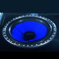
Stroboscope Light for Subwoofers and Low Frequency Speakers
This is a brand new invention illuminating subwoofer speaker and allowing the spectator to see the rhythm and customizable speaker movement! The device is used to illuminate the subwoofer in an (car) audio system. By analyzing audio signal it enhances the visual rhythm of the speaker and could be us...
...
Dual Stream Device/ Statistical Data Tracker
An Interactive Web-feed/television broadcast dual display system that enables a user to access any information currently available on the Internet without disrupting a television broadcast he/she may be currently watching. Web-based content is selected at the will of the viewer and is displayed on a...
...
Microwave Oven with Grill Function of Grilling with Slate Stone Slab
Hi, this patent is being concession in the patent office in Spain, with number of Application No.: 201230304 has vindication date and preference rights MARCH 20, 2012. Has until March 20 to present internationally worldwide PCT.
STATE OF THE ART
A microwave is an appliance used for heating fo...
...
Active Cooling System for LED Fixtures/ Electronics
MP Lighting's patented Active Cooling System (ACS) uses a thermal sensor, known as an NTC Thermistor Array, to detect changes in temperature and control speeds of a cooling fan. The system helps to regulate airflow through high-watt LED fixtures and other electronics, ensuring that the product opera...
...
Metamaterial Microwave Lens
A metamaterial microwave lens having an array of electronic inductive capacitive cells in which each cell has an electrically conductive pattern which corresponds to incident electromagnetic radiation as a resonator. At least one cell has a first and second electrical sections insulated from each ot...
...
Chemical Sensors and Methods for Making and Using the Same
A van der Pauw (VDP) sensor comprising an electronic circuit electrically coupled to a surface, the surface comprising a type III-V material, and the electronic circuit measuring a sheet resistivity of the surface using a VDP technique. The VDP sensor may further comprise a macromolecule, such as a ...
...
Implantable System for Restoring Accommodation Capacity Using Internal Energy
An implantable system for restoring accommodation capacity includes at least one ring configured to be implanted in a ciliary sulcus and a capacitor with a first capacitor plate and a second capacitor plate. The first capacitor plate is arranged on an implantable ring and the second capacitor plate ...
...
Method and Arrangement for Electrically Contacting an Object Surrounded By a Membrane, Using an Electrode
The invention relates in particular to a method for electrically contacting a membrane-object (30) with an electrode (10, 100).According to the invention is provided that is used for contacting at least one electrode (100) with a conductive carrier (110), on which a plurality of nano-needles (120) i...
...
Microarray-based Spatial Filter
The invention relates to a spatial filter measuring arrangement (1) and a spatial filter measuring device (2) comprising at least one sensor (4, 5; 41I - 41IV; 51) and a spatial filter, wherein electromagnetic radiation, in particular light, that is emitted or reflected by a measurement object (13),...
...
Multilayer circuit, particularly three-dimensional ceramic substrate system, is made of sintered ceramic material, where active electronic component is arranged in cavity
The multilayer circuit, particularly three-dimensional ceramic substrate system, is made of a sintered ceramic material. An active electronic component of a micro-system technology or Microelectromechanical systemor microelectronic is made of semiconducting material. The active electronic component ...
...
Completely Self-adjusted Surface-emitting Semiconductor Laser for Surface Mounting Having Optimized Properties
The present invention relates to a surface-emitting semiconductor laser having a vertical resonator, comprising a substrate base section (1) and a mesa (M) arranged on and/or at the substrate base section, the mesa substantially comprising, viewed perpendicular to the substrate base section: at leas...
...
Semiconductor device and method for manufacturing a semiconductor device
The invention concerns a semiconductor device (1) comprising a structure, wherein the structure comprising a substrate (8), a first layer (2) onto the substrate comprising GaN and a second layer (3) comprising AlGaN. The second layer is deposited onto the first layer and the first and the second lay...
...
Angled Junction Between a Microstrip Line and a Rectangular Waveguide
The present invention relates, in the field of radio-frequency engineering, to a junction element for transferring an electromagnetic wave in a strip conductor to a waveguide. In this case, a waveguide having a first opening is applied to a substrate, on which strip conductors and strip conductor st...
...
Thermal Diode Device and Methods
A thermal diode comprising a superlyophobic surface, and a lyophilic surface separated from the superlyophobic surface defining a chamber. A liquid is disposed in the chamber, the liquid capable of phase changing during operation of the thermal diode. Methods of cooling and insulating bodies and rec...
...
Sensors Incorporating Antibodies and Methods of Making and Using the Same
A sensor comprising an electronic circuit electrically coupled to a type II1-V semiconductor material, for example indium arsenide (InAs) and an antibody contacting the type II1-V semiconductor material. The sensor produces measurable changes in the electrical properties of the semiconductor upon an...
...
Method, Computer Program Product and System for the Tick Synchronization of Nodes in a Wireless Multi-hop Network
The invention relates to a method for the tick synchronization of a node of a wireless multi-hop network with at least one other node of said multi-hop network, said network comprising a plurality of nodes being arbitrarily connected, said method comprising the steps of: receiving a synchronization ...
...
Method for evaluating analyte
In an analyte evaluation method for evaluating an analyte, AC voltage is applied between a substrate electrode (2) on a substrate (4) and a counter electrode (8), and signals obtained from a marker (3) provided on an analyte bound to the substrate electrode are observed, wherein the frequency of the...
...
Circuit arrangement i.e. monolithic integrated circuit, has earth surfaces working as ground potentials for electrical and electronic circuits and as antenna units, where signal currents and antenna c
The arrangement has earth surfaces (31, 32) working as ground potentials for electrical and electronic circuits and as antenna units, where the circuits are connected with one another on or below the earth surfaces through conductors (L1, LM, LM+1, LN). Signal currents and antenna control currents a...
...
Method for Evaluating Target Molecule
In this method for evaluating a target molecule bonded to a probe molecule including a marker, an AC voltage is applied between a substrate electrode provided on a substrate and a counter electrode, and by using a signal obtained from the marker included on the probe molecule bonded to the substrate...
...
System and Methods for Dynamic Power Estimation for a Digital Circuit
A method for dynamic timing-dependent power estimation for a digital circuit having coupled interconnects and at least two gates. In one embodiment, the method includes the steps of capturing information on relative switching activities and timing dependence for the coupled interconnects in the digi...
...
On Wire Lithography-based Molecular Transport Junctions
On- wire lithography (OWL) fabricated nanogaps are used to construct molecular transport junctions (MTJs) through the assembly of molecular wires across a nanogap formed between two gold electrodes. Also disclosed are methods of characterizing a MTJ and optimizing gap size for two molecular wires of...
...
Organic Light-emitting Diodes and Methods for Assembly and Emission Control
New organic light-emitting diodes and related electroluminescent devices and methods for fabrication, using siloxane self-assembly techniques....
...
Carbonyl-Functionalized Thiophene Compounds and Related Device Structures
Carbonyl-functionalized oligo/polythiophene compounds, and related semiconductor components and related device structures....
...
Solution-processed High Mobility Inorganic Thin-film Transistors
Fluid media comprising inorganic semiconductor components for fabrication of thin film transistor devices....
...
Silole-Based Polymers and Semiconductor Materials Prepared from the Same
The present teachings provide silole-based polymers that can be used as p-type semiconductors. More specifically, the present teachings provide polymers that include a repeating unit of Formula I: wherein R1, R2, R3, R4, R5R6, Z, x, and x' are as defined herein. The present teachings also provide me...
...
Self-assembled Organic Monolayers on Graphene and Methods of Making and Using
Self-assembled organic monolayers on epitaxial graphene are described. The organic molecules are perylene derivatives including 3,4,9,10-perylene-tetracarboxylic dianhydride (PTCDA) molecules arranged in a herringbone phase and/or molecules are of the following formula: wherein R1 and R2 are alkyl g...
...
PNP light emitting transistor and method
A semiconductor light-emitting transistor device, including: a bipolar pnp transistor structure having a p-type collector, an n-type base, and a p-type emitter; a first tunnel junction coupled with the collector, and a second tunnel junction coupled with the emitter; and a collector contact coupled ...
...
Transistor Device and Method
A field-effect transistor device, including: a semiconductor heterostructure comprising, in a vertically stacked configuration, a semiconductor gate layer between semiconductor source and drain layers, the layers being separated by heterosteps; the gate layer having a thickness of less than about 10...
...
Stretchable and Foldable Electronic Devices
Disclosed herein are stretchable, foldable and optionally printable, processes for making devices and devices such as semiconductors, electronic circuits and components thereof that are capable of providing good performance when stretched, compressed, flexed or otherwise deformed. Strain isolation l...
...
Stretchable Form of Single Crystal Silicon for High Performance Electronics on Rubber Substrates
The present invention provides stretchable, and optionally printable, semiconductors and electronic circuits capable of providing good performance when stretched, compressed, flexed or otherwise deformed. Stretchable semiconductors and electronic circuits of the present invention preferred for some ...
...
Method of Fabricating a Planar Semiconductor Nanowire
A composition comprises a semiconductor substrate having a crystallographic plane oriented parallel to a surface of the substrate and at least one planar semiconductor nanowire epitaxially disposed on the substrate, where the nanowire is aligned along a crystallographic direction of the substrate pa...
...
Surface Preparation for Thin Film Growth by Enhanced Nucleation
Various processes and related systems are provided for making structures on substrate surfaces. Disclosed are methods of making a structure supported by a substrate by providing a substrate having a receiving surface and exposing at least a portion of the receiving surface to output from a remote pl...
...
Signal Processors, Signal Processing Methods, and Digital Filter Configuration Methods
Signal processors, signal processing methods, and digital filter configuration methods are discussed. In one arrangement, a signal processor includes a common node; a plurality of channels, each channel of the plurality comprising an analog filter, a sampler, and a digital filter and each channel of...
...
Medium Scale Carbon Nanotube Thin Film Integrated Circuits on Flexible Plastic Substrates
The present invention provides device components geometries and fabrication strategies for enhancing the electronic performance of electronic devices based on thin films of randomly oriented or partially aligned semiconducting nanotubes. In certain aspects, devices and methods of the present inventi...
...
Patterning Methods for Stretchable Structures
Described herein are processing techniques for fabrication of stretchable and/or flexible electronic devices using laser ablation patterning methods. The laser ablation patterning methods utilized herein allow for efficient manufacture of large area (e.g., up to 1 mm2 or greater or 1 m2 or greater) ...
...
Method of Plasma Etching Ga-based Compound Semiconductors
A method of plasma etching Ga-based compound semiconductors includes providing a process chamber and a source electrode adjacent to the process chamber. The process chamber contains a sample comprising a Ga-based compound semiconductor. The sample is in contact with a platen which is electrically co...
...
Methods and Devices for Fabricating and Assembling Printable Semiconductor Elements
The invention provides methods and devices for fabricating printable semiconductor elements and assembling printable semiconductor elements onto substrate surfaces. Methods, devices and device components of the present invention are capable of generating a wide range of flexible electronic and optoe...
...
Method of Forming a Nanoscale Three-demensional Pattern in a Porous Semiconductor
A method of forming a nanoscale three-dimensional pattern in a porous semiconductor includes providing a film comprising a semiconductor material and defining a nanoscale metal pattern on the film, where the metal pattern has at least one lateral dimension of about 100 nm or less in size. Semiconduc...
...
Light Emitting and Lasing Semiconductor Devices and Methods
A semiconductor light emitting device, including: a heterojunction bipolar light-emitting transistor having a base region between emitter and collector regions; emitter, base, and collector electrodes for coupling electrical signals with the emitter, base, and collector regions, respectively; and a ...
...
Light Emitting and Lasing Transistor Devices and Methods
A method for producing light emission from a semiconductor device includes the following steps: providing a semiconductor base region disposed between a semiconductor emitter region and a semiconductor collector region that forms a tunnel junction adjacent the base region; providing, in the base reg...
...
Light Emitting Semiconductor Methods and Devices
A method for producing light emission from a two terminal semiconductor device with improved efficiency, includes the following steps: providing a layered semiconductor structure including a semiconductor drain region comprising at least one drain layer, a semiconductor base region disposed on the d...
...
Method and System Having Adjustable Analog-To-Digital Conversion Levels
An adaptive Analog to Digital Converter (ADC) that adjusts the representation levels used in the conversion process so as to optimize system performance. By establishing system performance criteria by which to select or adjust the signal value range associated with each digital representation and/or...
...
Method of Forming an Array of High Aspect Ratio Semiconductor Nanostructures
A new method for forming an array of high aspect ratio semiconductor nanostructures entails positioning a surface of a stamp comprising a solid electrolyte in opposition to a conductive film disposed on a semiconductor substrate. The surface of the stamp includes a pattern of relief features in cont...
...
Hybrid Plasma-semiconductor Optoelectronic Devices and Transistors
The invention provides combination semiconductor and plasma devices, including transistors and phototransistors. A preferred embodiment hybrid plasma semiconductor device has active solid state semiconductor regions; and a plasma generated in proximity to the active solid state semiconductor regions...
...
Semiconducting Microcavity and Microchannel Plasma Devices
Preferred embodiments of the invention provide semiconducting microcavity plasma devices. Preferred embodiments of the invention are microcavity plasma devices having at least two pn junctions, separated by a microcavity or microchannel and powered by alternate half-cycles of a time-varying voltage ...
...
Light emitting and lasing semiconductor devices and methods
A two terminal semiconductor device for producing light emission in response to electrical signals, includes: a terminal-less semiconductor base region disposed between a semiconductor emitter region and a semiconductor collector region having a tunnel junction adjacent the base region; the base reg...
...
Semiconductor Heterostructure Nanowire Devices
Nanowire devices comprising core-shell or segmented nanowires are provided. In these nanowire devices, strain can be used as a tool to form metallic portions in nanowires made from compound semiconductor materials, and/or to create nanowires in which embedded quantum dots experience negative hydrost...
...
Pparatus and Semiconductor Co-crystal
The invention provides a method to enforce face-to-face stacking of organic semiconductors in the solid state that employs semiconductor co-crystal formers (SCCFs), to align semiconductor building blocks (SBBs). Single-crystal X-ray analysis reveals [pi]-orbital overlap optimal for organic semicondu...
...
Adaptive Mirror and Method for the Production Thereof
The invention relates to an adaptive mirror based on a ceramic substrate comprising a corresponding reflector and piezoelectric actuators, a cooling device being built into the substrate. The invention also relates a method for producing such a mirror. Said mirror can be used for the modulatation or...
...
Photosensitive Semiconductor Component
In a semiconductor device (1) with a photosensitive doped semiconductor layer (2), are released into the at absorption of electromagnetic radiation (6) electrical charge carriers, the photosensitive semiconductor layer (2) a structured interface (7).The structured interface (7) is at least one layer...
...
Detection Beyond the Standard Radiation Noise Limit Using Spectrally Selective Absorption
High sensitivity thermal detectors that perform beyond the blackbody radiation noise limit are described. Thermal detectors, as described herein, use spectrally selective materials that absorb strongly in the wavelength region of the desired signal but only weakly or not at all in the primary therma...
...
Soft Switching Power Electronic Transformer
This patent document discloses power electronic transformers having a high-frequency link. An example apparatus include a transformer having a primary winding and a secondary winding, the transformer is configured to receive a primary power signal having a first frequency, a primary converter config...
...
Method of Detecting and Correcting a Prescribed Set of Error Events Based on Error Detecting Code
A method of constructing an effective generator polynomial for error correction by which a unique set of syndromes for each error event is produced is provided. The method includes preparing a set of dominant error events from the intersymbol interference characteristics of media; and generating a c...
...
Device for Amplifying Light Pulses
The invention relates to a device (1, 11) for amplifying light pulses (2, 12), comprising a stretcher (4, 14) that temporally stretches the light pulses (2, 12), at least one amplifier (5, 15) that amplifies the stretched light pulses (2, 12), and a compressor (6, 16) that recompresses the stretched...
...
Device for Amplifying Light Impulses
The present invention relates to a device (12) and to a method for amplifying light impulses (13). The device comprises a stretcher (15) stretching the light impulses over time, at least one amplifier (16) amplifying the stretched light impulses, and a compressor (17) compressing the stretched and a...
...
I-III-VI2 Photovoltaic Absorber Layers
The invention provides a film having a composition AgWCu1-WInrGaxKySe2(I-Z)Q2Z; wherein K is Al or Tl or a combination of these; Q is S or Te or a combination of these; w is in a range from 0.01 to 0.75; x is in a range from 0.1 to 0.8; and r, y and z are each independently in a range from 0 to 1, p...
...
Eo Polymer-based Dual Slot Waveguide Modulators
Electro-optic modulators are disclosed. An electro-optic modulator comprises an electro-optic polymer layer, semiconductor layers, ferroelectric material layers, and electrodes. The semiconductor layers are positioned on each surface of the electro-optic polymer layer. The refractive index of the se...
...
Horizontally Depleted Metal Semiconductor Field Effect Transistor
The present invention provides a horizontally depleted Metal Semiconductor Field Effect Transistor (MESFET). A drain region, a source region, and a channel region are formed in the device layer such that the drain region and the source region are spaced apart from one another and the channel region ...
...
Epitaxial Methods and Templates Grown By the Methods
This invention provides methods for fabricating substantially continuous layers of a group III nitride semiconductor material having low defect densities and optionally having a selected crystal polarity. The methods include epitaxial growth nucleating and/or seeding on the upper portions of a plura...
...
Methods for Producing Improved Epitaxial Materials
This invention provides methods for fabricating substantially continuous layers of group III nitride semiconductor materials having low defect densities. The methods include epitaxial growth of nucleation layers on a base substrate, thermally treatment of said nucleation layer and epitaxial growth o...
...
IC Disabling Circuit
Systems and methods for disabling a secure Integrated Circuit (IC) are provided. In general, in response to detecting an event such as an intrusion on the secure IC, a supply voltage (VDD) node of the secure IC is clamped to, or effectively short circuited to, a reference voltage (Vss) node of the s...
...
Lattice Matched Multi- Junction Photovoltaic and Optoelectronic Devices
The present invention provides semiconductor structures comprising a substrate and at least three III-V and/or II- VI multi-junction building blocks, each comprising a p-n junction having at least two alloy layers, formed over the substrate, provided at least one multi-junction building block compri...
...
Methods for Improving the Quality of Group III-nitride Materials and Structures Produced By the Methods
The invention provides methods which can be applied during the epitaxial growth of two or more layers of Group Ill-nitride semiconductor materials so that the qualities of successive layer are successively improved. In preferred embodiments, surface defects interact with a protective layer of a prot...
...
Assemblies and Methods for Reducing Warp and Bow of a Flexible Substrate During Semiconductor Processing
Methods are described for addressing the bowing and/or warping of flexible substrates, attached to a rigid carrier, which occurs as a result of the thermal challenges of semiconductor processing. In particular, viscoelastic adhesives are provided which can bond a flexible substrate to a rigid carrie...
...
GeSn Infrared Photodetectors
Photodiode devices with GeSn active layers can be integrated directly on p+ Si platforms under CMOS-compatible conditions. It has been found that even minor amounts of Sn incorporation (2 %) dramatically expand the range of IR detection up to at least 1750 nm and substantially increases the absorpti...
...
Thin Group IV Semiconductor Structures
Thin group IV semiconductor structures are provided comprising a thin Si substrate and a second region formed directly on the Si substrate, where the second region comprises either (i) a Ge1-xSnx layer; or (ii) a Ge layer having a threading dislocation density of less than about 105/cm2, and the eff...
...
Hybrid Group IV/III-V Semiconductor Structures
Described herein are semiconductor structures comprising (i) a Si substrate; (ii) a buffer region formed directly over the Si substrate, wherein the buffer region comprises (a) a Ge layer having a threading dislocation density below about 105 cm-2; or (b) a Ge1-xSnx layer formed directly over the Si...
...
Methods for Attaching Flexible Substrates to Rigid Carriers and Resulting Devices
Flexible substrates can be temporarily attached to a rigid carrier for processing a surface thereof by depositing a joining material at one or more contact points between a flexible substrate and a rigid carrier, contacting the flexible substrate and the rigid carrier at the one or more contact poin...
...
Methods and System for Electrostatic Discharge Protection of Thin-film Transistor Backplane Arrays
The present invention provides devices and methods for testing the electrical performance of thin- film transistor backplane arrays and protecting thin- films during testing and handling....
...
Methods and System for On-chip Decoder for Array Test
The present invention provides devices capable of testing the electrical performance of thin- film transistor backplane arrays and methods for their use....
...
Four-terminal Soi Mesfet Based Low Dropout Regulator
Embodiments of a Low Dropout (LDO) regulator are provided in which an n-channel Metal Semiconductor Field Effect Transistor (MESFET) is utilized as a pass transistor of the LDO regulator. In one embodiment, the LDO regulator is implemented on an integrated circuit die and includes an n-channel Semic...
...
Integrated Circuits Secure from Invasion and Methods of Manufacturing the Same
An integrated circuit device that is secure from invasion and related methods are disclosed herein. Other embodiments are also disclosed herein....
...
Method of Etching Organosiloxane Dielectric Material and Semiconductor Device Thereof
In some embodiments, a method of etching an organosiloxane dielectric material can include: (a) providing the organosiloxane dielectric material; (b) providing a patterned mask over the organosiloxane dielectric material; and (c) reactive ion etching the organosiloxane dielectric material. Other emb...
...
Method of Providing a Semiconductor Device with a Dielectric Layer and Semiconductor Device Thereof
In some embodiments, a method of providing a semiconductor device can include: (a) providing a substrate; (b) depositing a first metal layer over the substrate; (c) spin-coating a first dielectric material over the first metal layer, where the first dielectric material includes an organic siloxane -...
...
Laterally Varying Ii-vi Alloys and Uses Thereof
Described herein are semiconductor structures comprising laterally varying II-VI alloy layer formed over a surface of a substrate. Further, methods are provided for preparing laterally varying II-VI alloy layers over at least a portion of a surface of a substrate comprising contacting at least a por...
...
Methods and compositions for preparing Ge/Si semiconductor substrates
The present disclosure describes methods for preparing semiconductor structures, comprising forming a Ge layer on a semiconductor substrate using an admixture of (a) (GeH3)2CH2 and Ge2H6; (b) GeH3CH3 and Ge2H6; or (c) (GeH3)2CH2, GeH3CH3 and Ge2H6, wherein in all cases, Ge2H6 is in excess. The discl...
...
Methods and compositions for preparing tensile strained Ge on Ge1-ySny buffered semiconductor substrates
The present disclosure describes methods for preparing semiconductor structures, comprising forming a Ge1-ySny buffer layer on a semiconductor substrate and forming a tensile strained Ge layer on the Ge1-ySny buffer layer using an admixture of (GeH3)2CH2 and Ge2H6 in a ratio of between 1:10 and 1:30...
...
Flexible Circuits and Electronic Textiles
Embodiments of wearable flexible devices and related methods are described herein. Other embodiments and related methods are also disclosed herein....
...
Amplifiers with Depletion and Enhancement Mode Thin Film Transistors and Related Methods
In one embodiment, an apparatus comprises an integrated circuit comprising an amplifier. The amplifier can comprise a first transistor over a substrate of the integrated circuit, and a second transistor over the substrate and coupled to the first transistor. The first transistor can comprise a first...
...
Method and apparatus for sampling and predicting rare events in complex electronic devices, circuits and systems
The invention provides methods for enhancing circuit reliability under statistical process variation. For highly replicated circuits such as SRAMs and flip flops, a rare statistical event for one circuit may induce a not-so-rare system failure. To combat this, the invention discloses the method call...
...
Method and Apparatus for Applying "Quasi-Monte Carlo" Methods to Complex Electronic Devices Circuits and Systems
The invention discloses a "Quasi-Monte Carlo" method originally intended for computational finance applications and applies said method to statistical circuit analysis. In doing so, it provides a means to efficiently and effectively detect and/or predict relatively rare failures or events to a wide ...
...
Direct Bandgap Substrates and Methods of Making and Using
An indirect bandgap thin film semiconductor circuit can be combined with a compound semiconductor LED such as to provide an active matrix LED array that can have high luminous capabilities such as for a light projector application. In another example, a highly efficient optical detector is achievabl...
...
Single-shot Semiconductor Processing System and Method Having Various Irradiation Patterns
High throughput systems and processes for recrystallizing thin film semiconductors that have been deposited at low temperatures on a substrate are provided. A thin film semiconductor workpiece is irradiated with a laser beam to melt and recrystallize target areas of the surface exposed to the laser ...
...
High-performance Gate Oxides Such As for Graphene Field-effect Transistors Or Carbon Nanotubes
An apparatus or method can include forming a graphene layer including a working surface, forming a polyvinyl alcohol (PVA) layer upon the working surface of the graphene layer, and forming a dielectric layer upon the PVA layer. In an example, the PVA layer can be activated and the dielectric layer c...
...
Method of Doping Organic Semiconductors
A method includes the steps of forming a contiguous semiconducting region and heating the region. The semiconducting region includes polyaromatic molecules. The heating raises the semiconducting region to a temperature above room temperature. The heating is performed in the presence of a dopant gas ...
...
Collections of Laterally Crystallized Semiconductor Islands for Use in Thin Film Transistors
Collections of laterally crystallized semiconductor islands for use in thin film transistors and systems and methods for making same are described. A display device includes a plurality of thin film transistors (TFTs) on a substrate, such that the TFTs are spaced apart from each other and each inclu...
...
Systems and Methods for Non-periodic Pulse Partial Melt Film Processing
In one aspect, the present disclosure relates to a method of processing a thin film including, while advancing a thin film in a first selected direction, irradiating a first region of the thin film with a first laser pulse and a second laser pulse, each laser pulse providing a shaped beam and having...
...
Asynchronous Digital Circuits Including Arbitration and Routing Primitives for Asynchronous and Mixed-timing Networks
Asynchronous digital circuits are described, including arbitration and routing primitives for asynchronous and mixed-timing networks. An asynchronous arbitration primitive has two data inputs and one data output. A mutual exclusion element is used to select the first-arriving data request from one o...
...
Hollow waveguide used in medicine and in structural analysis comprises a channel structure having an inner coating with a specified thickness
Hollow waveguide comprises a channel structure having an inner coating with a thickness of less than 50 nm. An independent claim is also included for a method for the production of the hollow waveguide....
...
Electromagnetic field distribution determining robot system for gigahertz transverse electromagnetic cell, has sensor suspended at flexible clamping elements that are connected with drive for specifyi
The system has a positioning device with a drive for positioning a sensor. The sensor is suspended at two flexible clamping elements e.g. wire. The clamping elements are connected with the drive in a region of ends of the drive for specifying effective element length, where the ends turn towards the...
...
Magneto-optoelectronic switch and sensor
A Magneto-Optoelectronic Device MOD (10) includes a magnetic sensing device (12), such as a magnetoresistive device or a magnetic tunnel junction device, that is combined with a semiconductor light emitter (14), such as a LED or a laser diode, to create a compact integrated device where changes in a...
...
Space-Charge-Free Semiconductor and Method
A semiconductor having a an n-type material and a p-type material, wherein the n-type material and p-type material are joined to form a space-charge-free p-n junction. The energy of the Fermi-level of the n-type material is equal to the energy of the Fermi-level of the p-type material. This allows f...
...
Semiconductor Device and Method
The present invention is directed to a semiconductor device that includes at least one p-n junction including a p-type material, an n-type material, and a depletion region. The at least one p-n junction is configured to generate bulk photocurrent in response to incident light. The at least one p-n j...
...
Transparent Rectifying Metal/metal Oxide/semiconductor Contact Structure and Method for the Production Thereof and Use
The invention relates to transparent rectifying contact structures for application in electronic devices, in particular appertaining to optoelectronics, solar technology and sensor technology, and also a method for the production thereof. The transparent rectifying contact structure according to the...
...
Functionalized, Hydrogen-passivated Silicon Surfaces
This invention is generally related to a method of making a molecule-surface interface comprising at least one surface comprising at least one material and at least one organic group wherein the organic group is adjoined to the surface and the method comprises contacting at least one organic group p...
...
Electronic Switching, Memory, and Sensor Devices from Carbon Sheets on Dielectric Materials
Electronic devices comprising a dielectric material, at least one carbon sheet, and two electrode terminals are described herein. The devices exhibit non-linear current-versus-voltage response over a voltage sweep range in various embodiments. Uses of the electronic devices as two- terminal memory d...
...
Vertically-stacked Electronic Devices Having Conductive Carbon Films
Vertically-stacked electronic devices having conductive carbon films are disclosed. The vertically-stacked devices exhibit non-linear current-versus-voltage response over a voltage sweep range in various embodiments. The vertically-stacked devices may be assembled into arrays where the vertically-st...
...
Integrated Embedded Processor Based Laser Spectroscopic Sensor
A novel low-power and compact laser spectroscopic sensor is described herein. Embodiments of the disclosed sensor utilize state-of-the-art microprocessors and digital processing techniques to reduce power consumption and integrate functions into a small device. In particular, novel software methods ...
...
Semiconducting Nanocrystals Comprising a Metal Sulfide Shell and Methods for their Preparation
Methods for synthesizing a semiconductor nanocrystal are provided comprising providing a semiconductive core; providing a metal precursor solution comprising a metal acetate, a non-polar solvent, trioctylphosphine, and trioctylphosphine oxide; providing a sulfur precursor solution; admixing the semi...
...
Fabrication of light emitting film coated fullerenes and their application for in-vivo emission
A nanoparticle coated with a semiconducting material and a method for making the same. In one embodiment, the method comprises making a semiconductor coated nanoparticle comprising a layer of at least one semiconducting material covering at least a portion of at least one surface of a nanoparticle, ...
...
Apparatus and Method for Compressive Imaging and Sensing Through Multiplexed Modulation
Compressive imaging apparatus employing multiple modulators in various optical schemes to generate the modulation patterns before the signal is recorded at a detector. The compressive imaging apparatus is equally valid when applying compressive imaging to structured light embodiments where the place...
...
Electronic Devices Containing Switchably Conductive Silicon Oxides as a Switching Element and Methods for Production and Use Thereof
In various embodiments, electronic devices containing switchably conductive silicon oxide as a switching element are described herein. The electronic devices are two-terminal devices containing a first electrical contact and a second electrical contact in which at least one of the first electrical c...
...
Method for Fabrication of a Semiconductor Element and Structure Thereof
Re-programmable antifuses and structures utilizing re-programmable antifuses are presented herein. Such structures include a configurable interconnect circuit having at least one re-programmable antifuse, wherein the at least one re-programmable antifuse is configured to be programmed to conduct by ...
...
Staggered Composition Quantum Well Method and Device
A light emitting device comprising a staggered composition quantum well....
...
Motion Activated Amplifier
An electronic device that includes a motion activated amplifier structured to receive a first DC signal having a first DC voltage level and output a second DC signal having a second DC voltage level that is greater than the first DC voltage level. The motion activated amplifier includes a motion act...
...
Methods and Apparatus for Switching a Transponder to an Active State, and Asset Management Systems Employing Same
A transponder that may be used as an RFID tag includes a passive circuit to eliminate the need for an "always on" active RF receiving element to anticipate a wake-up signal for the balance of the transponder electronics. This solution allows the entire active transponder to have all circuit elements...
...
Intelligent Modeling and Control of Automation
A system and method for advanced device specific knowledge based modeling as well as intelligent control to yield high performance, low cost automation for optoelectronic design, packaging and assembly. The control loop design is based on knowledge based model predictive control. A knowledge model, ...
...
Pyromellitic Diimide Organic Semiconductors and Devices
n-type organic semiconductors have a pyromellitic diimide structure and electronic or electro-optic devices include pyromellitic diimide compounds as organic semiconductors. Specific semiconductors include pyromellitic diimide compounds have sidechains comprising fluorine substituted aliphatic or ar...
...
Power Junction Field Effect Power Transistor with Highly Vertical Channel and Uniform Channel Opening
A semiconductor vertical junction field effect power transistor formed by a semiconductor structure having top and bottom surfaces and including a plurality of semiconductor layers with predetermined doping concentrations and thicknesses and comprising at least a bottom layer as drain layer, a middl...
...
Method for improved DEMON analysis using sub-band signals and local areas
The method involves subdividing a time-frequency-plane (9) into local regions (10), and separately evaluating demodulation of envelope modulation on noise (DEMON) spectrums, where each individual spectral value (11) consists of frequency and time points. Information carrying local regions of the spe...
...
Measuring Method and Device for Characterizing a Semiconductor Component
The invention relates to a measuring method for characterizing a semiconductor component (1) having at least one pn junction and a measuring surface, which is the front and/or rear of the semiconductor component and which has at least one contacting subarea, which is covered by a metallization or is...
...
Method for Fast Macropore Etching in N-type Silicon
Electrochemical etching of macropores in n-type silicon wafers under illumination of wafer's rear side by use of an aqueous electrolyte, is claimed, where the electrolyte is an aqueous acetic acid solution of a composition comprising water:acetic acid in a ratio of 2:1 and 7:3 with a mixture of at l...
...
Method and Arrangement for Reconstructing the Source of an Electromagnetic Field
The invention relates to a method for reconstructing the source (10, 23, 25) of an electromagnetic field. First, a measuring chamber (14) separate from the source (10, 23, 25) is selected so that the measuring space (14) is connected to the source (10, 23, 25) by means of a magnetically homogeneous ...
...
Electrode for Lithium-ion Accumulators
The invention relates to electrodes for lithium-ion accumulators comprising a metal film that is inert in relation to lithium ions and a plurality of silicon nanowires projecting from the film at least on a flat side of the film. Parts of the nanowires are surrounded by the metal film....
...
Apparatus Designed As a Robot for the Autonomous, Unmanned Determination of Leaks Releasing Substances Into the Surroundings from Pressurized Systems, Particularly Pipe Systems, and Method for Operati
The invention relates to an apparatus designed as a robot for the autonomous, unmanned determination of leaks releasing substances into the surroundings from pressurized systems, particularly pipe systems, said apparatus comprising a motor-operated movement platform, such as a chassis, having a sens...
...
Device for Subjecting Single- Or Three-phase Voltage Source to Parallel Operation By Equal Rating
PROBLEM TO BE SOLVED: To provide a device wherein two or more inductively coupled inverters are subjected to parallel operations by an equal rating, and therefor, any additional synchronizing line and/or communicating line are unnecessary. ; SOLUTION: In the device, each inverter has a controlling c...
...
Sensor Arrangement
The invention relates to a sensor having a conductor arrangement and an intervening dielectric to detect local sensor impedances in response to external forces. The conductor arrangement comprises elongate conductor strips between which the intervening dielectric is arranged as a compressible insula...
...
Method for Detecting Objects
The invention relates to a method for detecting objects, in which method a plurality of trajectory points are detected and evaluated together. According to the invention, the trajectory points are detected at least three-dimensionally and a plurality of three-dimensional measured values are evaluate...
...
Stacked Organic Photosensitive Devices
A device is provided having a first electrode, a second electrode, a first photoactive region having a characteristic absorption wavelength lambda1 and a second photoactive region having a characteristic absorption wavelength lambda2. The photoactive regions are disposed between the first and second...
...
Organic Photosensitive Devices
The present invention generally relates to organic photosensitive optoelectronic devices. More specifically, it is directed to organic photosensitive optoelectronic devices having a photoactive organic region containing encapsulated nanoparticles that exhibit plasmon resonances. An enhancement of th...
...
Oleds Doped with Phosphorescent Compounds
Organic light emitting devices are disclosed which are comprised of a heterostructure for producing electroluminescence wherein the heterostructure is comprised of an emissive layer containing a phosphorescent dopant compound. For example, the phosphorescent dopant compound may be comprised of plati...
...
Organometallic Complexes As Phosphorescent Emitters in Organic Leds
Organic light emitting devices are described wherein the emissive layer comprises a host material containing an emissive molecule, which molecule is adapted to luminesce when a voltage is applied across the heterostructure, and the emissive molecule is selected from the group of phosphorescent organ...
...
Organic Photosensitive Devices Using Subphthalocyanine Compounds
An organic photosensitive optoelectronic device, having a donor-acceptor heterojunction of a donor-like material and an acceptor-like material and methods of making such devices is provided. At least one of the donor-like material and the acceptor-like material includes a subphthalocyanine, a subpor...
...
Organic Light Emitting Devices Having Carrier Transporting Layers Comprising Metal Complexes
Light emitting devices having charge transporting layers comprising one or more metal complexes are provided. More particularly, devices include hole transporting layers comprising at least one metal complex are disclosed. The present devices can further comprise an electron blocking layer for impro...
...
Organic Light-emitting Device with a Phosphor-sensitized Fluorescent Emission Layer
The present invention relates to organic light emitting devices (OLEDs), and more specifically to OLEDS that emit light using a combination of fluorescent emitters and phosphorescent emitters. The emissive region of the devices of the present invention comprise at least one phosphor-sensitized layer...
...
Organic Triodes with Novel Grid Structures and Method of Production
An organic semiconductor device is provided. The device has a first electrode and a second electrode, with an organic semiconductor layer disposed between the first and second electrodes. An electrically conductive grid is disposed within the organic semiconductor layer, which has openings in which ...
...
System and Method for Depositing Thin Layers on Non-Planar Substrates by Stamping
An elastomeric stamp is used to deposit material on a non-planar substrate. A vacuum mold is used to deform the elastomeric stamp and pressure is applied to transfer material from the stamp to the substrate. By decreasing the vacuum applied by the vacuum mold, the elasticity of the stamp may be used...
...
Organic Photovoltaic Devices
The present invention generally relates to organic photosensitive optoelectronic devices. More specifically, it is directed to organic photovoltaic devices, e.g., organic solar cells. Further, it is directed to an optimized organic solar cell comprising multiple stacked subcells in series. High powe...
...
Semiconductor Coated Microporous Graphene Scaffolds
A high surface area scaffold to be used for a solar cell, made of a three- dimensional percolated network of functionalized graphene sheets. It may be used in the preparation of a high surface area electrode by coating with a semi conductive material. Electronic devices can be made therefrom, includ...
...
Non-crystalline Materials Having Complete Photonic, Electronic, Or Phononic Band Gaps
The invention provides an article of manufacture, and methods of designing and making the article. The article permits or prohibits waves of energy, especially photonic/electromagnetic energy, to propagate through it, depending on the energy band gaps built into it. The structure of the article may ...
...
Organic Photosensitive Optoelectronic Device Having a Phenanthroline Exciton Blocking Layer
An organic photosensitive optoelectronic device, having an anode, a cathode, and an organic blocking layer between the anode and the cathode is described, wherein the blocking layer comprises a phenanthroline derivative, and at least partially blocks at least one of excitons, electrons, and holes....
...
Organic photosensitive optoelectronic device
The invention relates to a mixed electrical configuration stacked organic photosensitive optoelectronic device comprising a substrate having a proximal surface and a distal surface and plurality of subassemblies of organic photosensitive optoelectronic subcells, each of said subcells having a cathod...
...
Hybrid Layers for Use in Coatings on Electronic Devices Or Other Articles
A method for protecting an electronic device comprising an organic device body. The method involves the use of a hybrid layer deposited by chemical vapor deposition. The hybrid layer comprises a mixture of a polymeric material and a non-polymeric material, wherein the weight ratio of polymeric to no...
...
Very high efficiency organic light emitting devices based on electrophosphorescence
The invention relates to an organic light emitting device comprising an anode, a cathode, and an emissive layer, wherein the emissive layer is located between the anode and the cathode, and the emissive layer comprises a phosphorescent organometallic compound, wherein the phosphorescent organometall...
...
Method of fabricating devices by stamping
The invention relates to a method of fabricating an organic device, comprising: depositing a first organic layer onto a patterned, soft elastomeric stamp; and transferring the first organic layer from the patterned, soft elastomeric stamp onto a substrate....
...
Controlled growth of larger heterojunction interface area for organic photosensitive devices
An optoelectronic device and a method of fabricating a photosensitive optoelectronic device includes depositing a first organic semiconductor material on a first electrode to form a continuous first layer having protrusions, a side of the first layer opposite the first electrode having a surface are...
...
Hybrid Dielectric Material for Thin Film Transistors
Thin-film transistors are made using a hybrid silica-silicone material as an insulating material. The hybrid silica-silicone material may be deposited by plasma-enhanced chemical vapor deposition from siloxanes and oxygen. These hybrid materials may be employed as the gate dielectric, as a subbing l...
...
High Efficiency Multi-color Electro-phosphorescent Oleds
The present invention relates to efficient organic light emitting devices (OLEDs) doped with multiple light-emitting dopants, at least one dopant comprising a phosphorescent emitter, in a thin film emissive layer or layers. The present invention is directed to an efficient phosphorescent organic lig...
...
Printed Electronics
Printed electronic device comprising a substrate onto at least one surface of which has been applied a layer of an electrically conductive ink comprising functionalized graphene sheets and at least one binder. A method of preparing printed electronic devices is further disclosed....
...
Sensors
The invention provides sensors that are useful for detecting and measuring chemical characteristics and physical properties of compositions containing analytes. The invention further provides, among other things, methods for making the sensors and for using them, as well as modified cells having sen...
...
Bistable Nanoswitch
A non-volatile bistable nano-electromechanical switch is provided for use in memory devices and microprocessors. The switch employs carbon nanotubes as the actuation element. A method has been developed for fabricating nanoswitches having one single-walled carbon nanotube as the actuator. The actuat...
...
Large Scale Nanoelement Assembly Method for Making Nanoscale Circuit Interconnects and Diodes
Nanoelements such as single walled carbon nanotubes are assembled in three dimensions into a nanoscale template on a substrate by means of electrophoresis and dielectrophoresis at ambient temperature. The current-voltage relation indicates that strong substrate-nanotube interconnects carrying mA cur...
...
System and Method for Coupling a Multi-mode Optical Fiber to a Single Mode Optical Fiber
A multi-mode to single mode optical interface device includes an optically pumped edge emitting semiconductor laser device and a lens. The optically pumped edge emitting semiconductor laser device includes (1) a gain area, and (2) an edge located single mode output. The lens focuses a multi-mode opt...
...
Multiple Excitation Capacitance Polling for Enhanced Electronic Capacitance Tomography
Disclosed herein is a novel sensing technique, termed Multiple Excitation Capacitance Polling (MECaP), that improves the efficiency of Electrical Capacitance Tomography (ECT). Unlike traditional alternating current techniques, where excitation signal is applied to an electrode one at a time, MECaP i...
...
Thyristor radiation detector array and applications thereof
An array of thyristor detector devices is provided having an epitaxial growth structure with complementary types of modulation doped quantum well interfaces located between a P+layer and an N+ layer. The thyristor detector devices operate over successive cycles that each include a sequence of two di...
...
Low-temperature Surface Doping/alloying/coating of Large Scale Semiconductor Nanowire Arrays
A method and corresponding system for providing a uniform nanowire array including uniform nanowires composed of at least three elements is presented. An embodiment of the method includes growing an array of two-element nanowires, and thereafter uniformly doping or alloying each two-element nanowire...
...
Device and Method for Measurement
Substances either separated or not by means of 1D or 2D flat bed electrophoresis or chromatography can be directly measured without pre-marking, by means of measuring the fluorescence thereof in the UV region with a UV detector, the above being stimulated by means of irradiation with UV light in the...
...
Method for Stabilizing a Laser Beam
The invention relates to a method for stabilizing a laser beam, which performs a reciprocating movement about a pivot point, at an examination location, in which the pivot point (D1) of the reciprocating movement is projected onto the examination location (D2) by means of an arrangement having at le...
...
Method and Apparatus for Stabilizing a Laser Beam
The invention relates to a method for stabilizing a laser beam, in particular for stabilizing the profile intensity and/or the pendulum motion, in which an initial laser beam (1) is split into two partial beams (2, 3), wherein the two partial beams (2, 3) are rotated relative to one another by 180 d...
...
Layer system based on a high magnetic field or semiconductor-hybrids, comprises layers of a half-metallic ferromagnet, in an alternating arrangement, and a semiconducting compound, or a semiconducting
Layer system based on high magnetic field/semiconductor-hybrids, comprises one or more layers of a half-metallic ferromagnet, in an alternating arrangement, and a semiconducting compound, or a semiconducting non-stoichiometric compound. Layer system based on a high magnetic field/semiconductor-hybri...
...
Non-wettable Surfaces
An object having a surface that has: filaments having a length of from 30 to 6000 [mu]m, a diameter to length ratio of from 1:10 to 1:20, and are bound to the surface with at least one front face thereof; wherein the distance between two neighboring filaments on the surface is such that the ratio of...
...
Optical Devices Featuring Nonpolar Textured Semiconductor Layers
A semiconductor emitter, or a precursor therefor, has a substrate and one or more textured semiconductor layers deposited onto the substrate in a nonpolar orientation. The textured layers enhance light extraction, and the use of nonpolar orientation greatly enhances internal quantum efficiency compa...
...
Chemical/biological Sensor Employing Scattered Chromatic Components in Nano-patterned Aperiodic Surfaces
A label-free multiplexed sensing platform is based on light interaction with aperiodic photonic structures with an advantage of a broadband operation. Multiple-scattering-induced "fingerprinting" colorimetric signatures can be used as a transduction mechanism. Aperiodic sensing platforms can operate...
...
Glucose Sensor Employing Semiconductor Nanoelectronic Device
A glucose sensor employs a programmable glucose sensor array of a relatively large number of nanoelectronic devices (e.g. semiconductor field-effect devices) having control surfaces functionalized with a glucose-reactive substance and generating sensing signals indicative of sensed glucose level of ...
...
Biological Circuit Chemotactic Converters
Described herein are novel biological circuit chemotactic converter that utilize modular components, such as genetic toggle switches and single invertase memory modules (SIMMs), for detecting and converting external inputs, such as chemoattractants, into outputs that allow for autonomous chemotaxis ...
...
Biological Analog-to-digital and Digital-to-analog Converter Switches
Described herein are novel biological converter switches that utilize modular components, such as genetic toggle switches and single invertase memory modules (SIMMs), for converting analog inputs to digital outputs, and digital inputs to analog outputs, in cells and cellular systems. Flexibility in ...
...
Nanochannel-based Sensor System with Controlled Sensitivity
Disclosed are sensors, devices, systems, arrays of sensors and methods, including a sensing device that includes a sensor including one or more nanochannels constructed from semiconductor material and connected at their opposite ends to electrodes, the one or more nanochannels having at least one el...
...
Device for Amplifying And/or Transporting Electromagnetic Radiation
The invention relates to a device (1) for amplifying and/or transporting electromagnetic radiation, comprising a radiation source (2) for generating the electromagnetic radiation and an amplifier (4) for amplifying or a medium for transporting the generated electromagnetic radiation. In order to mak...
...
Sers Substrate
The invention relates to a novel SERS substrate, a method for the production thereof, a method for the examination thereof, and the use thereof. The aim of the invention, which is to provide novel SERS substrates that can be produced in a cost-effective manner compared to clean-room SERS substrates ...
...
Bragg mirror with superlattice for compensation of lattice mismatch
The semiconductor element (10) has a layer pair (11) with a layer (12) having refractive index and a lattice constant. Another layer (13) has another refractive index which is different from the former refractive index. The former layer is formed as a super lattice (23) by different periodically rep...
...
Manufacturing semiconductor device for use as gas sensor, photo-detector, photo cell, solar cell, diode or light emitting diode, involves forming seed layer on nano-wire layer by using solution in pre
Semiconductor device manufacturing involves forming seed layer on nano-wire layer by using a solution at 30, preferably 100, particularly 200[deg] C in a pressure tank at a pressure of 14.5 bars. An independent claim is also included for a semiconductor device, which comprises a p-type zinc oxide na...
...
Bipolar Transistor with Quantum Well Base and Quantum Well Emitter
A double heterojunction bipolar transistor (DHBT) is disclosed having a quantum well base and a quantum well emitter. The energy band profile of a DHBT can be used t create a quantum well for holes and a quantum barrier for electrons....
...
Field Effect Transistor with Independently Biased Gates
A field effect transistor (FET) having at least two independently biased gates can provide uniform electric field in the channel region of the FET. The same AC voltage may be applied to each gate for modulating the FET. One of the gates is positioned closer to the channel region than the other gate....
...
Field Effect Transistor with Shifted Gate
A field effect transistor has a shifted gate such that the gate-source distance depends on the ratio of the threshold voltage to the drain voltage. In one embodiment, a switch may include two FETs: one FET in a series configuration and one FET in a shunt configuration. Providing a switch having at l...
...
Improved Complementary Metal Oxide Semiconductor Devices
Improvements in Complementary Metal Oxide Semiconductor (CMOS) devices; in particular, field effect transistors (FETs) and devices using said transistors which are able to take advantage of the higher carrier mobility of electrons compared to holes by replacing the conventional p-channel transistor ...
...
Ferroelectric Devices Including a Layer Having Two Or More Stable Configurations
Ferroelectric semiconductor devices are provided by including a ferroelectric layer in the device that is made of a material that is not ferroelectric in bulk. Such layers can be disposed at interfaces to promote ferroelectric switching in a semiconductor device. Switching of conduction in the semic...
...
Pwm Amplifier
Amplifier device of the pulse width modulation amplifier type (PWM amplifier), which comprises a switch according to a micro-electromechanical system (MEMS-switch) for a signal to be amplified (Vi), wherein the MEMS switch comprises at least one substrate (1) on which are arranged - a movable thin f...
...
Method for Improvement of Semiconductor Crystalline Lattice
The invention applies to field of technical physics, and it can be used in electronics and optoelectronics. In invention it is shown that there is a possibility to improve semiconductor crystalline lattice. High gradient of temperature has the main role in this process, and interstitial atoms and va...
...
Pyrene-based Polymers for Organic Light Emitting Diodes (oleds )
The present invention relates to novel pyrene-based polymers, methods of preparing the same and uses thereof, in particular for electroluminescent devices. The novel polymers of the invention have the following general formula (I): wherein R1, R2, R3, R4, R5, R6, R7 and R8 are independently of each ...
...
OFET-based sensor for detecting an analyte
An electrical sensor ("SensFET") is provided for qualitatively and/or quantitatively detecting an analyte of interest (molecules, ions etc.) in a gaseous or liquid medium, comprising an organic field-effect transistor device fabricated on a rigid or flexible substrate (61) having a source electrode ...
...
Motion Estimation and Compensation Process and Device
In the motion estimation and compensation process for video frames, blocks O of pixels are considered. A number k of bit planes in a block O in a video frame F are compared with blocks OR in reference frames (FR). The best matching block (ORM) is determined in the reference frames (FR). Subsequently...
...
Method for Providing a Crystalline Germanium Layer on a Substrate
The present invention provides a method for providing a crystalline germanium layer on a crystalline base substrate having a crystalline surface. The method comprises cleaning the base substrate for removing contaminants and/or native oxides from the surface, providing an amorphous germanium layer o...
...
Switchable Multiband LNA Design
A low noise amplifying (LNA) circuit comprising an amplifying section (11, 12) and a feedback means (14) arranged for providing input matching from the output to the input. The LNA circuit further comprises at least one frequency band determining inductor (15) having a predetermined resonance freque...
...
Interleaved Pipelined Binary Search A/d Converter
The present invention is related to a pipelined analog-to-digital converter, ADC, for converting an analog input signal into a digital signal comprising - a plurality of comparing means having tuneable thresholds for comparing an input signal with; at least two of said given thresholds being differe...
...
Devices for emitting radiation with a high efficiency
The present invention aims to disclose radiation, preferably light emitting, devices with a high radiation emission efficiency. The invention further aims at disclosing radiation, preferably light, emitting devices that can be fabricated as small devices in an array of such devices. In a first objec...
...
Photonic Mixer
The photonic mixer for use in time of flight (TOF) applications comprises substrate 1 having a field area that is doped with a dopant of a first conductivity type; a couple of an injecting contact region 3 for injecting the majority carrier-current into the semiconductor substrate 1 and a detector r...
...
Sigma-delta-based analog-to-digital converter
An analog to digital converting device is proposed for generating a digital output signal of an RF analog input signal. The device comprises a first analog to digital converter stage, a mixer, a second analog to digital converter stage and a digital filter. The first analog to digital converter stag...
...
Stretchable Electronic Device
A stretchable electronic device comprising a stretchable interconnection electrically connecting two electronic components, the stretchable interconnection comprising an electrically conductive channel having a predetermined first geometry by which said channel is stretchable up to a given elastic l...
...
Photon Induced Removal of Copper
Preferred embodiments provide a method for removing at least part of a copper comprising layer from a substrate, the substrate comprising at least a copper comprising surface layer. The method comprises in a first reaction chamber converting at least part of the copper comprising surface layer into ...
...
Method and Apparatus for Determining the Junction Depth of a Semiconductor Region
A method of determining a value of a depth of a semiconductor junction of a substrate using a photomodulated optical reflectance measurement technique is disclosed. In one aspect, the method includes obtaining a substrate which has at least a first region including the semiconductor junction. The me...
...
Solution Processing Method for Forming Electrical Contacts of Organic Devices
The present invention relates to a method for forming, on an organic semiconductor layer, an electrical contact layer comprising a metal, the method comprising the steps of: (a) providing a charge collecting barrier layer on the organic semiconductor layer; (b) providing a liquid composition compris...
...
Method for Performing Parallel Stochastic Assembly
A method of positioning at least 2 chips simultaneously on a substrate by parallel stochastic assembly in a first liquid, wherein the chips are directed to target sites on the substrate within the first liquid, the target sites being covered with a second liquid, the second liquid and the first liqu...
...
Method for determining the doping profile of a partially activated doped semiconductor region
A method is disclosed for determining the inactive doping concentration of a semiconductor region using a PMOR method, the method comprising: providing a set of at least two semiconductor regions having substantially the same known as-implanted concentration but known varying junction depth, determi...
...
Scalable Quantum Well Device and Method for Manufacturing the Same
A quantum well device and a method for manufacturing the same are disclosed. In one aspect, the device includes a quantum well region overlying a substrate, a gate region overlying a portion of the quantum well region, a source and drain region adjacent to the gate region. The quantum well region in...
...
Method for fabricating a dual workfunction semiconductor device and the device made thereof
A method for manufacturing a dual work function semiconductor device and the dual work function semiconductor device made thereof is described. The method comprises providing a semiconductor substrate; providing a gate dielectric layer (104) on and in contact with the semiconductor substrate; formin...
...
Organic Non-volatile Memory Device
The invention relates to an organic memory element comprising an organic semiconductor material, a gate dielectric stack comprising a first dielectric layer acting as a barrier layer and a second dielectric layer of an organic material, and a gate electrode. The gate electrode is separated from the ...
...
Determining Active Doping Profiles in Semiconductor Structures
An optical measurement method and system is disclosed to determine an active doping profile of a semiconductor substrate, the method comprising directing at least one pump laser pulse of a pump laser beam on the semiconductor substrate, with at least one pump laser pulse having a pump laser pulse po...
...
Method for Forming Mems Variable Capacitors
A method for fabricating an out-of-plane variable overlap MEMS capacitor comprises: providing a substrate (40) comprising a first layer (41), a second layer (42), and a third layer (43) stacked on top of one another; and etching a plurality of first trenches (70) through the third layer (43), throug...
...
Semiconductor Package
A semiconductor package which comprises a base frame and a wiring substrate mounted on the base frame. The base frame comprises two pieces made of a material with respectively a first and a second coefficient of thermal expansion and connected to each other via resilient connecting structures. The w...
...
Method for Insertion Bonding and Device Thus Obtained
A method for insertion bonding and a device thus obtained are disclosed. In one aspect, the device includes a first substrate having a front main surface and at least one protrusion at the front main surface. The device includes a second substrate having a front main surface and at least one hole ex...
...
Method for Encapsulating a Device in a Microcavity
Manufacturing a semiconductor device involves forming (200) a sacrificial layer where a micro cavity is to be located, forming (210) a metal layer of thickness greater than 1 micron over the sacrificial layer, forming (220) a porous layer from the metal layer, the porous layer having pores of length...
...
Method of Forming Mono-Crystalline Germanium or Silicon Germanium
A method is presented for forming mono-crystalline germanium or silicon germanium in a trench. In an embodiment, the method comprises providing a substrate comprising at least one active region that is adjacent to two insulating regions, forming in the active region a trench having a width of less t...
...
Large Time Constant Steering Circuit and Instrumentation Amplifier Implementing Same
The present invention relates to a large time constant steering circuit for slowly changing a voltage on a node between at least two discrete voltage levels. The present invention further relates to a slow steering current DAC comprising said large time constant steering circuit. The present inventi...
...
Method of manufacturing a semiconductor device and semiconductor devices resulting therefrom
A method is disclosed for manufacturing a semiconductor device, the method comprising - providing a substrate comprising a main surface with a non flat topography, the surface comprising substantial topography variations; - forming a first capping layer over the main surface; wherein, during formati...
...
Memory Circuit with Multi-sized Sense Amplifier Redundancy
A memory circuit with multi-sized sense amplifier redundancy is disclosed. In one aspect, the circuit includes sense amplifiers connected to differential bit-lines and configured to amplify a voltage difference sensed on the differential bit-lines. The sense amplifiers include a first set of smaller...
...
Dipyrannylidene Derivatives As an Anode Interfacial Layer in Electronic Devices
The present invention relates to substrates coated with films including compounds having the following generic formula (I): formula (I) as well as the manufacturing method thereof and the use of same as an anode interfacial layer in electronic devices. The present invention also relates to organic l...
...
Tunnel Nanowire Transistor
The invention provides a new type of transistor comprising a nanowire structure adapted to provide a tunnel barrier such that an applied gate voltage causes a current to oscillate, as the gate voltage is increased, to provide a region of negative transconductance. The device presents oscillations of...
...
Junctionless Metal-oxide-semiconductor Transistor
A junctionless metal-oxide-semiconductor transistor is described. In one aspect, a transistor device comprises a semiconductor material. The semiconductor material comprises first, second, and third portions. The second portion is located between the first and third portions. The first, second, and ...
...
A semiconductor optical amplifier with a reduced noise figure
A semiconductor optical amplifier 100 comprises an input for receiving the optical signal 102 and an output for outputting an amplified version of the optical signal. A semiconductor active medium 107 defines an amplification path between the input and the output for amplifying the optical signal as...
...
Electronic Cleansing of Digital Data Sets
A method of processing a 3-dimensional Computed Tomography Colonography data set to remove tagged material is disclosed. The method involves the preliminary processing step of classifying voxels in the data set as corresponding to air, tagged material or colon tissue. Methods of overcoming erroneous...
...
A New Type of Gapless Semiconductor Material
The present disclosure provides a new type of gapless semiconductor material having electronic properties that can be characterized by an electronic band structure which comprises valence and conduction band portions VB1 and CB1, respectively, for a first electron spin polarisation, and valence and ...
...
Spectrum Sliced Photonic Signal Processor
A photonic signal processor providing finite impulse response filtering of an external input signal, the processor including: a photonic signal input having a predetermined wavelength range, a Bragg grating structure interconnected to the photonic signal input and having a series of localised modifi...
...
Semiconductor Device Including Nanocrystals and Methods of Manufacturing the Same
The present invention relates generally to methods of manufacturing semiconductor devices with p-n junctions including nanocrystals, for instance, quantum-dot light emitting devices ('QD-LEDs'). The present invention also provides semiconductor devices such as, for instance, QD-LEDs which have been ...
...
Diffusely Radiating Led Light System
A lighting device (7) for illuminating objects, the lighting device comprising: a plurality of light emitting diodes (1) wherein at least one of the plurality of light emitting diodes is adapted to generate light having a spectrum different from a spectrum of light generated by another light emittin...
...
High efficiency power converter, and modulator and transmitter using it
The invention refers to a Digital to Analog converter able to manage a flow of forward and reverse energy, from source and load, through the control of two PWM (Pulse Width Modulator). This technique allows obtaining high efficiency as well as the fast dynamic of signals (about 30 kHz) up to zero vo...
...
System for Diagnosis and Treatment of Photovoltaic and Other Semiconductor Devices
A diagnostic and self-healing treatment system for a semiconductor device, the system provides: i) a shunt busting/blocking treatment, ii) self-healing treatment, and iii) an in-situ non-contact diagnostic determination....
...
Wireless apparatus with proximity sensor switches allowing a disabled person to control an electronic device.
Disclosed is a proximity sensor switch operated control unit for electronic devices to be used by disabled persons with limited motor skills. The control unit consists of switches that sends signals to electronic units which process the signals and send secondary signals wirelessly to a computing de...
...
A Receiver of Multiplexed Binary Offset Carrier (MBOC) Modulated Signals
A receiver for receiving a navigation signal comprising a carrier modulated by a code modulation function of a given code rate and further modulated by a composite sub-carrier modulation function having first and second components with two different rates both of which are different to the code rate...
...
Frame Timing and Carrier Frequency Recovery for Frequency Selective Signals
A method and apparatus is provided for rapid frame/symbol timing and carrier frequency synchronization of a digital receiver to an orthogonal frequency division multiplexing (OFDM) signal and other transmissions (either continuous or burst) over a frequency-selective (wideband) channel. The method m...
...
Doped Dielectric Layers and Method for Formation Thereof
A doped dielectric layer and a method for forming the doped dielectric layer are provided. The doped dielectric layer comprises (a) a silicon dioxide or silicon oxynitride layer (b) doped with from about 0.01 to about 20 atomic percent of one or more rare-earth elements, the one or more rare-earth e...
...
Light Emitting Semiconductor Device
A light emitting semiconductor device (401) has an active region (405) formed of Bismuth (Bi) and one or more othergroup V elements. In a particular embodiment the III-V material comprises Gallium Arsenide (GaAs) in addition to Bismuth. The inclusion of Bismuth in the III-V material raises the spin-...
...
Mounting Method
A mounting method is provided for mounting electric components on both faces of a substrate. Because the electric components 32, 33 on a front face and a rear face of the substrate 31 are simultaneously pressed with first and second pressing rubbers 15, 25, the electric components 32, 33 can be conn...
...
Light emitting diode and method for manufacturing the same
Provided are a light emitting diode (LED) and a method for manufacturing the same. The LED includes an n-type semiconductor layer, an active layer, and a p-type semiconductor layer. The active layer includes a well layer and a barrier layer that are alternately laminated at least twice. The barrier...
...
Light emitting diode with improved structure
Disclosed is a light emitting diode (LED) with an improved structure. The LED comprises an N-type semiconductor layer, a P-type semiconductor layer and an active layer interposed between the N-type and P-type semiconductor layers. The P-type compound semiconductor layer has a laminated structure com...
...
AC light emitting diode
Disclosed is a light emitting diode (LED) operated by being directly connected to an AC power source. An AC LED according to the present invention comprises a plurality of light emitting cells two-dimensionally arranged on a single substrate; and wires electrically connecting the light emitting cell...
...
Laser diode having nano patterns and method of fabricating the same
Disclosed is a laser diode having nano patterns. The laser diode has a substrate (21). A first conductive-type clad layer (35) is disposed over the substrate (21), and a second conductive-type clad layer (41) is disposed over the first conductive-type clad layer (35). An active layer (37) is interpo...
...
Resin Composition and Display Apparatus
A thin display unit that incorporates a high-luminance, high-contrast display part that is free of image defects caused by the deformation of the display part is provided. The display unit of the present invention includes an image display part 2 and a light-transmitting protective part 3 arranged o...
...
Wiring Board Receiving Plate, and Device and Method for Connection of Wiring Board Using Same
It is an object to realize ACF connection with a high connecting reliability that achieves uniform thermal compression bonding for a wiring board with electronic components mounted on the back surface. A thermal compression bonding head (12) presses flexible printed circuit boards (4, 5) against a m...
...
Video Encoding Decoding Method and Device and Video Codec
A video encoding decoding method and device and a video codec are provided. The video encoding method includes: the first view picture is basic layer encoded as a reference view picture, the predication information is extracted in combination with the second view picture and the second view picture ...
...
Video Camera Calibration Method and Device Thereof
Disclosed is a video camera calibration method. Intrinsic and extrinsic parameters of the video camera are acquired according to a reference template, and data of a reference object in a shooting scene is recorded. When it is necessary to calibrate the video camera, images of the reference object ar...
...
Light Emitting Device for AC Operation
An AC light emitting device is disclosed. The AC light emitting device includes at least four substrates. Serial arrays each of which has a plurality of light emitting cells connected in series are positioned on the substrates, respectively. Meanwhile, first connector means electrically connect the ...
...
Method, System, and Apparauts for Realizing Program Hidding
A method and system, apparatus thereof for realizing hidden program is disclosed. By way of obtaining a sub electronic program guide (EPG) identification, this method involves receiving total EPG sent by a total head-end, where the total EPG includes the sub EPG identification (ID) and the sub EPG w...
...
Dynamic Electronic Synapse Device
An electronic synapse device comprising a substrate formed from semiconductor material and a plurality of inputs including a first input for receiving a weighting signal and a second input for receiving a signal from a pre-synaptic neuron device. An insulating layer is provided between the inputs an...
...
Method, System and Device for Remote Control Terminal
A method for remote control terminal is disclosed in embodiments of the present invention, which used for device management (DM) system comprises the following steps: receiving a remote control command provided by a DM server, and the remote control command comprising access time (AT) command inform...
...
Light Emitting Diode Having Light Emitting Cell with Different Size and Light Emitting Device Thereof
There is provided a light emitting diode operating under AC power comprising a substrate; a buffer layer formed on the substrate; and a plurality of light emitting cells formed on the buffer layer to have different sizes and to be electrically isolated from one another, the plurality of light emitti...
...
Alternating current motor drive circuit and electric vehicle drive circuit
To eliminate a need for a large volumetric reactor in a direct current chopper, achieving a downsizing of the circuit. A current source rectifier is provided at an output of an alternating current generator, an alternating current motor is connected to an output of the rectifier via a voltage source...
...
Configurable Electronic Device and Method
A configurable transistor device comprising a primary transistor and at least one secondary transistors, said primary transistor and said secondary transistors having their drain electrodes connected to a common drain electrode and their source electrodes connected to a common source electrode, said...
...
Processing of Object Detection Signals
A method of processing return remote sensing pulses comprising using Bayes Linear statistics to modify a return remote sensing pulse in light of at least one of data relating to at least one previously processed return remote sensing pulse and data governing the return remote sensing pulse shape/par...
...
Semiconductor Optoelectronic Devices and Methods for Making Semiconductor Optoelectronic Devices
A semiconductor-based optoelectronic device such as a solar cell has an n-type layer and a p-type layer, together forming a p-n junction. Contact regions are formed on the device, with light-receiving regions between contact regions. A window layer is formed over the n-type layer or the p-type layer...
...
Frequency Reference Devices and Methods of Providing Frequency References
A frequency reference device has a population of atoms or ions held in a vapour cell providing a first frequency reference signal by virtue of at least one electronic transition. A driving means provides a driving signal to the population of atoms or ions to promote the electronic transition. A dete...
...
Wire Bond Free Connection of High Frequency Piezoelectric Ultrasound Transducer Arrays
A piezoelectric ultrasound transducer array connected to a planar electronic component, the planar electronic component having one or more through hole adapted to receive a conducting element to provide an electrical connection which extends through the planar electronic component....
...
Video Camera Calibration Method and Device Thereof
A method for calibrating the video camera includes: obtaining the internal and external parameters of the video camera according to a reference template; recording data of a reference object in the scene; obtaining images of the reference object from at least two perspectives; and obtaining the inte...
...
Magnetic Sheet
The present invention is aimed to provide a magnetic sheet, which is capable of suppressing undesirable electromagnetic waves emitted from an electronic equipment, inhibiting electromagnetic disorders caused by an interference of unnecessary electromagnetic waves within an electronic equipment, has ...
...
A Video Encoding/decoding Method and a Video Encoder/decoder
A video coding method, a video decoding method, a video coder, and a video decoder are disclosed herein. A video coding method includes: performing base-layer coding for the first view, and extracting prediction information of at least one layer by combining a locally decoded first view and a second...
...
Video Encoding Decoding Method and Device and Video Codec
A video encoding decoding method and device and a video codec are provided. The video encoding method includes the following steps. A first view picture is basic-layer encoded as a reference view picture, prediction information is extracted in combination with a second view picture, and the second v...
...
Patterning
The present invention provides a method of patterning an electronic or photonic material on a substrate comprising: forming a film of said electronic or photonic material on said substrate; and using a fluoropolymer to protect regions of said electronic or photonic material during a patterning proce...
...
Optoelectronic Devices
An optoelectronic device comprises electon donor D and acceptor A semiconducting species and an intervening co-oligomeric or copolymeric species provided to alter the energy transfer characteristics of excitons to or from the interface between the said electron acceptor and donor species. The interv...
...
Linear Mode-locked DFB-fiber Laser with Repetition Rate Control
An embodiment of the invention relates to a multi-segment all-fiber laser device (10). The device includes a first active fiber laser segment (20), a first grating (25), a second grating (35), and a gain-phase coupling fiber segment (40) arranged between the first and second gratings, said gain-phas...
...
Printed Electronic Device
This invention generally relates to a patterned substrate for an electronic device and to electronic devices, device arrays, field effect transistors and transistor arrays comprising the patterned substrate. The invention also relates to a logic circuit, display, memory or sensor device comprising t...
...
Microfluidic devices
A layer-by-layer deposition method for forming multiple layers of material onto the walls of a channel of a microfluidic device is disclosed. The method comprises: loading a tube with a series of segments of solution, a segment of solution bearing a material to be deposited; coupling the tube to the...
...
Signed up for selling some patents at your market place last week. Yesterday I recceived a contact from a serious and relevant company. Really impressed, thanks for a great service!
– Cristina C.