Doped Dielectric Layers and Method for Formation Thereof
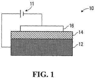
A doped dielectric layer and a method for forming the doped dielectric layer are provided. The doped dielectric layer comprises (a) a silicon dioxide or silicon oxynitride layer (b) doped with from about 0.01 to about 20 atomic percent of one or more rare-earth elements, the one or more rare-earth element being distributed throughout the dielectric layer. Semiconductor structures comprising the above dielectric layer are also provided.Attached files:
Patents:
WO 2,010,020,046
Inventor(s): KNIGHTS ANDREW P [CA]; HALSALL MATTHEW [GB]; GWILLIAM RUSSELL MARK [GB]
Type of Offer: Sale
« More Electronics Patents