Non-crystalline Materials Having Complete Photonic, Electronic, Or Phononic Band Gaps
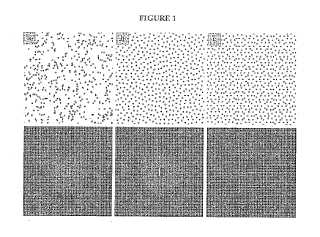
The invention provides an article of manufacture, and methods of designing and making the article. The article permits or prohibits waves of energy, especially photonic/electromagnetic energy, to propagate through it, depending on the energy band gaps built into it. The structure of the article may be reduced to a pattern of points having a hyperuniform distribution. The point-pattern may exhibit a crystalline symmetry, a quasicrystalline symmetry or may be aperiodic. In some embodiments, the point pattern exhibits no long-range order. Preferably, the point-pattern is isotropic. In all embodiments, the article has a complete, TE- and TM-optimized band-gap.; The extraordinary transmission phenomena found in the disordered hyperuniform photonic structures of the invention find use in optical micro-circuitry (all-optical, electronic or thermal switching of the transmission), near- field optical probing, thermophotovoltaics, and energy-efficient incandescent sources.Attached files:
Patents:
WO 2,011,005,530
Inventor(s): STEINHARDT PAUL J [US]; TORQUATO SALVATORE [US]; FLORESCU MARIAN [US]
Type of Offer: Licensing
« More Electronics Patents