Method of Forming Gated, Self-aligned Micro-structures and Nano-structures
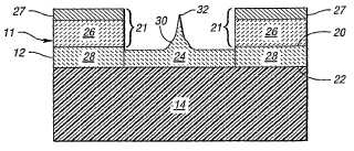
Methods of forming a gated, self-aligned nano-structures for electron extraction are disclosed. One method of forming the nano-structure comprises irradiating a first surface of a thermally conductive laminate to melt an area across the first surface of the laminate. The laminate comprises a thermally conductive film and a patterned layer disposed on the first surface of the film. The patterned layer has a pattern formed therethrough, defining the area for melting. The film is insulated at a second surface thereof to provide two-dimensional heat transfer laterally in plane of the film. The liquid density of the film is greater than the solid density thereof.; The method further comprises cooling the area inwardly from the periphery thereof to form the nano-structure having an apical nano-tip for electron emission centered in an electrically isolated aperture that serves as a gate electrode to control electron extraction in a gated field emitter device.Attached files:

Patents:
US 20,090,142,936
Inventor(s): BAIRD RONALD J [US]; GEORGIEV DANIEL G [US]; AVRUTSKY IVAN [US]; NEWAZ GOLAM [US]; AUNER GREGORY W [US]
Type of Offer: Licensing
« More Nanotech Patents
« More Engineering - Electrical Patents