Methods for Producing Improved Epitaxial Materials
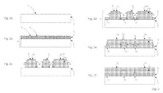
This invention provides methods for fabricating substantially continuous layers of group III nitride semiconductor materials having low defect densities. The methods include epitaxial growth of nucleation layers on a base substrate, thermally treatment of said nucleation layer and epitaxial growth of a discontinuous masking layer. The methods outlined promote defect reduction through masking, annihilation and coalescence, therefore producing semiconductor structures with low defect densities. The invention can be applied to a wide range of semiconductor materials, both elemental semiconductors, e.g., combinations of Si (silicon) with strained Si (sSi) and/or Ge (germanium), and compound semiconductors, e.g., group II-VI and group III-V compound semiconductor materials.Attached files:
Patents:
WO 2,009,015,337
Inventor(s): ARENA CHANTAL [US]; MAHAJAN SUBHASH [US]; DATTA RANJAN [US]
Type of Offer: Licensing
« More Electronics Patents