Direct-bandgap Nano-crystalline Optoelectronic Devices
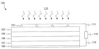
A photovoltaic device is provided comprising a thin-film of an energy conversion material. The energy conversion material includes one or more quantum structures, where the quantum structures comprise a semiconductor material having an indirect band-gap in the bulk. The average size of the quantum structures is selected such that a direct and an indirect band-gaps are modified in the semiconductor material such that the direct band-gap provides charge carrier generation when the quantum structures are exposed to light.Attached files:

Patents:
WO 2,010,057,994
Inventor(s): TIMMERMAN DOLF [NL]; GREGORKIEWICZ TOMASZ [NL]; DE BOER WIETEKE DINY ANTONIUS MARIA [NL]
Type of Offer: Sale
« More Energy Patents
« More Solar Patents
